MICROCHIP LASERS: Beyond the visible
PHILIPPE JURY
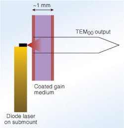
The microchip laser was first demonstrated in 1989 by MIT Lincoln Laboratory (Lexington, MA). The laser comprised a thin solid-state gain material placed between two flat, parallel dielectric mirrors and was pumped by a strongly localized diode-laser source; it was shown to be capable of single-mode laser emission if the gain-material thickness was thin enough (see Fig. 1). In 1993, passive Q-switching in microchip lasers was first demonstrated using a saturable-absorber material placed within the cavity, which was kept monolithic, thanks to diffusion-bonding of materials.
The typical cavity of a microchip laser is about a millimeter long, allowing for very compact lasers with surprising performance, such as subnanosecond pulse widths and a peak power of several tens of kilowatts. These remarkable properties allow high wavelength-conversion efficiency in nonlinear crystals. Companies rapidly commercialized microchip lasers not only for the infrared (1064 nm) fundamental wavelength, but also—by placing nonlinear crystals external to the cavity—for green (532 nm) in 1996, and for UV (355 and 266 nm) in 1998.
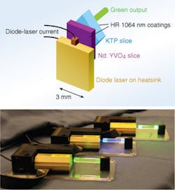
In parallel, intracavity frequency-doubled Nd:YVO4 (vanadate) lasers were demonstrated by the University of Saint Andrews (St. Andrews, Scotland) that emit tens to hundreds of milliwatts of continuous-wave (CW) red, green, and blue light (see Fig. 2). Low loss and small beam waist allowed the generation of significant circulating IR fields, and thus efficient second-harmonic generation inside the cavity.Intracavity harmonic generation of UV light was first achieved in early 2006 with the demonstration of 355 nm CW microchip lasers by Oxxius (Lannion, France), a company already known for its visible CW microchip lasers; this achievement is just one example of the latest advances in short-wavelength generation.
Industrial status
Early efforts by the first microchip-laser companies (Micracor, Uniphase, Litton, Sfim, Nanolase) involved difficult technical challenges and sometimes produced lasers that were perceived to be less than commercially ready. Though the microchip-laser concept is simple, developers need a very high level of know-how and expertise to master the technological subtleties.
Since the early times, microchip lasers (see "Microlaser versus microchip laser—a clarifying definition") have gained acceptance in the industry and are now recognized for their robustness, reliability, compactness, and unique capabilities. Thousands of microchip lasers have been produced by several companies, especially in Europe, at many different wavelengths. As an example, wavelengths that have been produced for Nd:YAG microchip lasers include 1320, 1122, 1064, and 946 nm in the fundamental; 660, 561, 532, and 473 nm with frequency doubling; and 355 and 266 nm in the UV.
UV passively Q-switched microchip lasersWith their high beam quality, pulsed UV microchip lasers can advantageously replace more-powerful gas lasers—such as nitrogen or helium cadmium (HeCd). As an example, a 355 nm microchip laser that produces 15 µJ pulses can replace a nitrogen laser with a 300 µJ pulse energy in some MALDI (matrix-assisted laser desorption/ionization) applications, with the additional benefit of a higher repetition rate. They are now largely used in applications like microdissection, MALDI, biohazard detection, photoluminescence-based semiconductor inspection, and others.
Three companies are most active in the field, two German—CryLas (Berlin) and Lumanova (Hannover)—and one French, Teem Photonics (Meylan). At first view, Teem Photonics could be viewed as the most recent company in the field, but in fact its product line results from the purchase in 2005 of JDS Uniphase's (Santa Rosa, CA) microchip laser business, which arose from the pioneering activities at Nanolase. Teem Photonics is the sole company that now offers subnanosecond pulse duration. Initial products have been improved over the years, especially by sealing the packages.
The MicroFlare product from Lumanova was developed more recently and was directly designed to be hermetically sealed using the latest packaging technology: as a result, the MicroFlare laser head is contained in a very compact butterfly package of 30 x 13 x 8 mm, well-suited for OEM integrators contending with severe constraints on size. The laser also has the highest repetition rate—up to 25 KHz—although with lower pulse energy of 0.2 µJ.
The output of CryLas microchip lasers, emitting either at 355 or 266 nm, is delivered via optical fiber, thanks to an SMA connector output. In a passive Q-switched laser, the user cannot easily change the pulse repetition rate: the pulse frequency is usually set at the factory as a function of pump power. External or internal triggering are ways to control the pulse emission, in which the laser pulse is emitted after each triggering demand, but after a certain time delay. External triggering (0 to 2 KHz) and internal triggering (30 Hz to 2 KHz) of both 266 and 355 nm CryLas microchip lasers are possible.
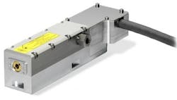
Similarly, Teem Photonics introduced at Photonics West 2007 a new 1064 nm microchip laser with a triggering capability between 10 Hz and 2 KHz, as well as a specified delay period between trigger demand and pulse emission time along this frequency range (see Fig. 3). This interesting feature will open new applications until now reserved to active Q-switched lasers.UV CW microchip lasers
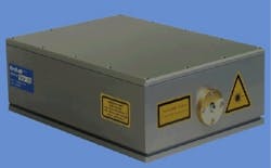
In the CW domain, two recent developments should be noted. In the first, Oxxius is pursuing the development of a truly monolithic microchip laser cavity emitting at 355 nm and will introduce the laser commercially in 2007. Second, CryLas introduced at Photonics West 2007 a new laser emitting up to 10 mW of 266 nm CW single-frequency light with an electrical-power consumption of less than 100 W (see Fig. 4).These are real breakthroughs, as most conventional CW UV lasers are cumbersome and have high power consumption, which makes their integration somewhat difficult for some OEM applications. The commercial availability of compact UV single-frequency sources emitting tens of milliwatts at 355 or 266 nm will open new application opportunities, especially those that rely on intrinsic laser-induced effects.
Perspectives
While external frequency conversion to 213 nm directly from the output of a pulsed microchip laser has been demonstrated in the laboratory, the low conversion efficiency—inherent to the cascade of several frequency-doubling and mixing operations (1064 doubled to 532 nm; 1064 and 532 nm mixed to 355 nm; and 532 and 355 nm mixed to 213 nm)—resulted in very low output power.
Several research laboratories are exploring an innovative solution: amplifying microchip-laser output with a fiber amplifier. Researchers at Clausthal University (Clausthal-Zellerfeld, Germany), for example, have demonstrated pulse energies of up to 1 mJ while maintaining a nanosecond pulse duration, high repetition rate, and good beam quality with fiber delivery. At 1064 nm, the result is a peak power of greater than 1 MW—opening up new applications to microchip lasers such as marking, material processing, and micro-LIBS (laser-induced-breakdown spectroscopy). The German researchers have demonstrated frequency conversion down to 213 nm.
In November 2006, groups at Sandia National Laboratories (Albuquerque, NM) and Teem Photonics published the results of a laboratory demonstration of a fiber-amplified microchip laser with a variable repetition rate (7 to 27 KHz), a pulse duration of 1 ns, and pulse energies up to 0.4 mJ. They demonstrated up to 0.14 W of emission at 213 nm. Applications of such 213 nm sources include particle diffraction, noncontact testing of integrated circuits, and replacement of low-power excimer lasers.
Microchip-laser technology is now mature and robust, with results that include nanosecond pulse durations and high peak power for pulsed lasers, as well as single frequencies and high stability for CW lasers. A large variety of wavelengths is available in the infrared and visible, while in the UV, several producers now offer high-reliability products with a variety of packages, outputs, and specifications. Laboratory demonstrations of Q-switched output at 213 nm have been demonstrated by Clausthal University (Clausthal, Germany), Sandia National Laboratories, and Teem Photonics. Recent market introductions (triggering capabilities, CW UV output) and the exciting developments toward high-power and short-wavelength laser emission will create new application opportunities in the near future.
Philippe Jury is president of Cohessence, 15 Rue du Pal de Fer, 38240 Meylan, France; e-mail: [email protected]; www.cohessence.com.


