JON S. LAPINGTON, PAUL. W. MAY, NEIL A. FOX, JON HOWORTH, and JAMES MILNES
In the last decade, numerous developments in diamond and diamond-like-carbon (DLC) films for applications in electronics, optics, and engineering have been reported, with multimillion dollar markets predicted. Diamond films have many attractive properties: they are hard, wear resistant, offer low friction, have high thermal conductivity, are electrically resistant and optically transparent over an unusually wide frequency range, and—crucially for our application—can have a negative-surface work function making them eminently suitable for cold-cathode emission for use in field-emission displays, and as highly efficient dynodes in photomultipliers.1
Advantages of diamond
Diamond can be deposited using chemical-vapor deposition (CVD) coating techniques, or nanocrystalline diamond grits can be ink-jet printed to form structures and patterns for selective film growth and as a feedstock for low-cost manufacture of conductive nanodiamond.2 Lithiated diamond grits can be used to produce a very low work function cathode material, and as micro-arrays, have potential applications in microvacuum electronic devices such as thermionic cathodes, microwave amplifiers, and space-borne sensors and displays.3
The application of diamond as a robust, stable, and cost-effective dynode material with improved secondary electron yield (SEY) for electron multiplication in vacuo will provide a fundamental enabling technology for the next generation of three-dimensional (3-D; time and position) photon and particle-counting detectors, crucial for continuing technological progress in a wide variety of diverse applications from the life sciences to particle physics, environmental monitoring, and astronomy.
Enhanced SEY results
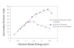
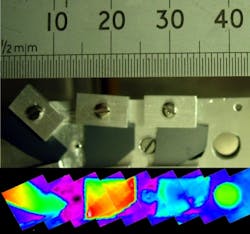
We have characterized the SEY of a variety of diamond samples from various sources, manufactured using different methods (CVD and ink-jet-printed nanoparticles), dopants and dopant concentrations, and differing crystallinities (see Fig. 1). The highest SEY value so far obtained—45 at 2.4 keV for B-doped diamond on silicon—is the highest reported for hydrogen-terminated material, and other surface terminations offer the potential for even higher SEY. Our characterization apparatus also allows the electron beam to be scanned to produce two-dimensional (2-D) images mapping the variation of SEY with position, and is used for dynode uniformity measurements (see Fig. 2).Diamond as dynode
Despite recent advances in the photon-counting capabilities of solid-state detectors using gain mechanisms such as the avalanche photodiode (APD) and its variants, the potential event-timing performance of vacuum-tube detectors remains unequalled. These devices, typified by the traditional photomultiplier tube (PMT) and microchannel plate detector, utilize in vacuo secondary electron emission as a gain mechanism. Primary electrons (either initial photoelectrons or subsequent secondary electrons) are accelerated by means of an electric field towards an electrode known as a dynode which is optimized for the production of secondary electrons. Secondary electrons produced in the material by the impact of primaries are ejected back into the vacuum to be accelerated and produce further amplification.
The choice of dynode material has a crucial bearing on many performance aspects of devices exploiting in vacuo electron gain. Synthetically deposited CVD diamond offers a number of significant advantages over traditional materials. One major attraction is its very high SEY, with reported values greater than 80 at 2.8 keV primary electron energy.4 This CVD diamond film can be boron (B) doped to make it conductive—a necessary attribute for a dynode—and its surface modified to produce negative electron affinity (NEA), a feature making ejection of secondary electrons from the surface energetically favorable and responsible for the high secondary yield.
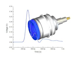
Higher dynode SEY offers several benefits for detectors. First, it improves the response time of the detector, which is controlled by the time transit spread (TTS), the range of times taken for electrons to traverse all gain stages. A device using high SEY dynodes requires a lower number of gain stages for a given signal level. And TTS, which is driven by energy and trajectory variability of secondary electrons, is reduced if the number of stages can be lowered. In addition, B-doped diamond films produce secondary electrons with a narrow energy distribution and low transverse energy, allowing easier confinement of electron trajectories, faster response, and reduced background.5 Lower TTS translates to high signal bandwidth in analog mode, or improved time resolution in event-counting mode. Event timing accuracy on the order of 10 ps is projected with simulated diamond dynode PMT designs. Lower dynode count is also a distinct advantage in terms of device size, cost, and complexity.
Second, a higher dynode SEY reduces the variance in output amplitude driven by the Poisson-like statistics of each gain stage. This translates to improved energy resolution, applicable to energy discrimination in positron-emission-tomography (PET) scanners, improved energy resolution for scintillators in high energy physics, x-ray imaging with energy resolution, or it can provide more accurate counting statistics and enhanced signal-to-noise performance where background is an issue.
And finally, diamond's wide bandgap of 5.47 eV virtually precludes thermal noise at room temperature, or conversely produces lower noise at elevated temperatures compared with conventional devices. Although other high band-gap materials such as aluminum nitride, boron nitride, and gallium nitride can exhibit NEA, CVD diamond does not require substrate lattice matching and can be deposited onto a conventional Si wafer.
Patterned and structured diamond coatings have already been demonstrated using various techniques such as micromachining, lithographic, and such printing processes as ink-jet printing, diamond-coated tungsten wire meshes, and free-standing micromeshes.6-8 In comparison with virtually all other high-gain dynode materials, diamond has a stable SEY minimally affected by long-term storage or exposure to air and can be restored by surface reactivation.9
Future goals
Our goals for the short term are to produce larger and faster triode designs and to demonstrate enhanced pulse-height distribution in a high-gain, super-fast PMT. In the medium term we have a program to develop imaging-diamond PMTs. This involves the development of a transmissive dynode, the first step in the manufacture of a multi-stage 2-D imaging PMT that will combine the high throughput of a conventional dynode-based device with the speed potential offered by diamond technology.
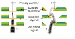
The transmissive dynode will comprise a 2-D array of miniature gain channels micromachined on a silicon substrate and has two potential modes of operation, transmission and reflection. In transmission mode, primary electrons enter and secondary electrons exit through opposite faces of a thin diamond film. Electron absorption and diffusion requires that the film thickness is either less than 100 nm, or that an internal drift field is used, allowing thicker films. In reflection mode, diamond is deposited on a porous, 3-D support substrate engineered so that the secondary electrons, produced from the same surface that the primaries impact, can exit the structure (see Fig. 4).Conceptually, the transmission technique is superior, providing linear propagation of signal through the detector for minimum TTS, guaranteed primary electron collision at the first dynode, freedom from electron-beam contamination effects, which degrade the NEA, and is ideally suited for 2-D imaging applications. However, despite its advantages, it also presents significant technological difficulties, and the choice between the two technologies will be a crucial milestone in our development program.
Transmissive electron-multiplication structures using diamond dynodes offer many advantages for the development of future photon- and electron-imaging detectors. We envisage detectors comprising arrays of miniature sensors, using fewer, higher-gain discrete dynode stages to provide enhanced energy and timing capabilities, and engineered as monolithic devices with the potential for vacuum encapsulation. Transmissive diamond dynode technology will enable a step change in photon-counting vacuum-tube technology, from traditional PMTs to imaging, large-area, flat-panel detector designs comprising micro-machined 2-D pixel arrays—a revolution analogous to the replacement of the cathode ray tube by today's flat-screen liquid-crystal displays.
REFERENCES
1. P.W. May, Philosophical Transactions of the Royal Society of London A 358, 473 (2000).
2. N.A. Fox et al., Diamond and Related Materials 9, 1263 (2000).
3. S.A. Furkert et al., Appl. Phys. Lett. 90, 242109 (2007).
4. J.E. Yater, A. Shih, and R. Abrams, Phys. Rev. B 56, R4410 (1997).
5. J.B. Miller and G.R. Brandes, J. Applied Physics 82, 4538 (1997).
6. N.A. Fox et al., J. Applied Physics 87, 8187 (2000).
7. E.D. Nicholson et al., Diamond and Related Materials 5, 658 (1996).
8. V.V. Dvorkin et al., Diamond and Related Materials 12, 2208 (2003).
9. G.T. Mearini, I.L. Krainsky, and J.A. Dayton Jr., Surface and Interface Analysis 21, 138 (1994).
Jon S. Lapington is senior research fellow in the Space Research Centre in the Department of Physics and Astronomy at the University of Leicester, University Road, Leicester LE1 7RH, England; email: [email protected]; www.le.ac.uk. Paul W. May is a reader in physical chemistry and Neil A. Fox is Great Western research fellow in wide bandgap nanomaterials in the School of Chemistry at the University of Bristol, Tyndall Avenue, Bristol BS8 1TH, England; www.bristol.ac.uk. Jon Howorth is director and James Milnes is a research engineer at Photek, 26 Castleham Rd., St. Leonards on Sea, East Sussex TN38 9NS, England.


