BRAD OSTMAN
Charge-coupled devices (CCDs) have been at the forefront of high-performance electronic imaging since the early 1970s. A number of articles over the last decade have predicted the demise of the CCD due to the rapid development and improvements in complementary metal-oxide semiconductor (CMOS) imaging. Yes, CMOS has joined the ranks of high-quality imagers and will replace the CCD for many imaging applications. However, certain key characteristics of the CCD, such as time delay and integration (TDI), will ensure that CCD is the technology of choice for specific applications for years to come.
The battle between CCD and CMOS for high-performance imaging dominance rages on. Last year, Fairchild Imaging, in collaboration with Andor Technology (Belfast, Northern Ireland) and PCO (Kelheim, Germany), launched Scientific CMOS (sCMOS) technology, which represents the state of the art in high-performance imaging and is in many ways superior to CCD technology. While sCMOS is widely predicted to replace the CCD, both technologies provide researchers and consumers with imaging solutions uniquely suited to individual application requirements. In digital-imaging segments where near-perfect cosmetics and noiseless charge transfer are deciding factors in image-sensor selection, CCD sensors will continue to dominate. One CCD architecture in particular continues to provide unsurpassed performance in particular cases. When the observation of a target requires synchronization due to image movement, a CCD technique known as time delay and integration (TDI) provides excellent image quality due to its unique method of capturing imagery.
TDI basics
In order to appreciate what makes the TDI CCD so effective, some basic fundamentals of how a TDI CCD operates are required. Time delay and integration is an old technique dating back to the age of film. It was developed for aerial reconnaissance to solve the problem of image smear and improve the signal-to-noise ratio (SNR). The essence of the technique is to leave the camera shutter open and roll the film at the same relative velocity as the target image thereby collecting a long strip of film of an apparently static scene. TDI offers several advantages: first, it eliminates the need for a mechanical shutter; second, it enables long exposure times without introducing smear. Finally, it allows capture of tremendous amounts of high-resolution imagery from a relatively small camera when compared to an equivalent framing camera.
The CCD with its noiseless charge transfer capability can implement the TDI method in a fashion completely analogous to the old film technique. Instead of rolling film, the registers of the CCD are clocked in synchronization with the object velocity—charge is "coupled" (hence charge-coupled device) from row to row in the sensor. Image signal integrates higher and higher as it traverses the sensor such that the final image is orders of magnitude brighter compared to an equivalent static image. A typical TDI CCD might have 64 rows enabling a 64x improvement in signal and an 8x improvement in SNR.
These TDI CCDs are the detector of choice in such diverse applications as letter and film scanning, aerial reconnaissance, digital radiography, and satellite mapping due to their sensitivity and large full-well capacity. Increased sensitivity allows signal detection at lower light levels. The larger full-well capacity provides high dynamic range unachievable with classic CCD and CMOS imagers.
Applications suited to TDI
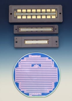
As one of the early pioneers in CCD development, Fairchild Imaging began supplying TDI CCDs in the late 1970s and has developed a family of TDI sensors ranging from 2K (2048 pixels) to 24K in length (see Fig. 1). The company has delivered tens of thousands of TDI CCDs in virtually every size for high-resolution scanning applications.
We recently supported the United States Postal Service with high-speed TDI CCD sensors for barcode reading and letter inspection. These devices feature 2048 resolution elements and 96 TDI lines vertical and run at a 100 MHz data rate. As pieces of mail move past the fixed scanner, TDI synchronization produces a final image without blur. And because of the increased sensitivity of the TDI CCD, the brightness of the illuminator is reduced, thereby extending the life of the system.
Larger-format TDI devices find their niches in aerial reconnaissance and space-imaging applications, where target images are in motion at fixed rates. The famous aerial reconnaissance platform, the U-2 spy plane, houses one of the most advanced high-resolution TDI imaging systems in the world. This camera, developed by Fairchild Imaging for the Goodrich Corporation, is part of the Senior Year Electro-Optical Reconnaissance System (SYERS), which provides continuous real-time imagery in both the visible and infrared. The SYERS system can collect imagery continuously in several wavebands to cut through haze and to make images in low-light conditions up to 100 nautical miles away with broad area coverage. The camera consists of three coplanar, parallel, TDI imagers stagger butted to provide 10,240 pixels in the cross-scan direction. Each of the imagers has 32 stages of TDI. Bandpass filters are included to provide the necessary color requirements. Color imagery, created by combining three visible bands, further reveals important clues to hidden or buried targets during analysis.
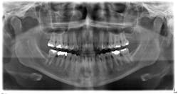
Space imaging of earth resources, and for mapping or surveillance, is also best served by large TDI imagers (see Fig. 2). These sensors provide very large swath widths, negligible image blur, require no image stitching, and offer excellent resolution. We recently delivered a 24,000 line multispectral TDI imager for KOMPSAT-3, an earth observation satellite developed by the Korean Aerospace Research Institute (KARI). Due to the size of the device, which exceeded the width of the silicon wafer needed to produce the sensor, two 12K devices were butted together to extend the length to over 8 inches of imaging area. This very large TDI imager supports KARI in gathering geographical, agricultural, and oceanographic image data for environmental monitoring applications.Today there are exciting choices in digital imaging. The maturation of CMOS is great news for many popular imaging applications. Yet it remains critical to assess the application and imaging requirements for which a sensor is to be used. Tradeoffs in sensor architecture complexity and sensor performance need to be understood when choosing the proper imaging technology. Though CMOS is making serious progress in image quality and is the right choice for many applications, TDI CCDs will continue to dominate the image-scanning trade space for the foreseeable future. For image capture of targets in low-light or in motion; from mail scanning to aerial reconnaissance; from digital dental radiography to satellite mapping; TDI CCD remains the technology of choice.
Brad Ostman is director of Aerospace Imaging at Fairchild Imaging, 1801 McCarthy Blvd., Milpitas, CA 95035; e-mail: [email protected]; www.fairchildimaging.com.


