TERAHERTZ SOURCES: Large-area photoconductive emitters improve terahertz source efficiency
THOMAS DEKORSY, JURE DEMSAR, STEPHAN WINNERL, MATTHIAS BECK, and GREGOR KLATT
Commercial terahertz spectrometers operating at frequencies from 0.1 to 3.0 THz are widely used in academic and industrial research labs. Most time-domain terahertz systems are based on terahertz generation via photoexcitation of photoconductive switches with femtosecond lasers and require highly efficient terahertz emitters in order to achieve good system performance. However, for many terahertz sources, long-term stability and high conversion efficiency is still lacking.
Two new concepts for terahertz generation overcome these problems. The first is a biased large-area photoconductive emitter with high conversion efficiency and the second concept is a new approach to the generation of intense terahertz radiation based on the photo-Dember effect—a technique that does not require a bias voltage. The large-area design of both concepts enables scalability toward high terahertz electric fields, enabling both high signal-to-noise ratios and short acquisition times.
Radiation from accelerated carriers
The common feature of both concepts is the emission of electromagnetic radiation from accelerated carriers in semiconductors like gallium arsenide (GaAs) or indium GaAs (InGaAs). Free carriers—electrons and holes—are generated at the surface of the semiconductor by femtosecond pulses with photon energy above the gap energy of the semiconductor (in our case we use 50 fs pulses at about 800 nm).
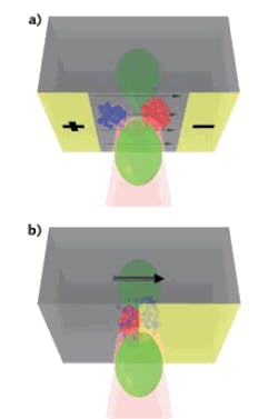
For conventional photoconductive switches, electrodes deposited on the substrate material are externally biased and hence an electric field occurs in between the electrodes. After photoexcitation, an electric dipole builds up when the photogenerated electrons and holes are separated in the electric field (see Fig. 1). Typically the electrons have a much higher mobility than the holes, so mainly the electrons are accelerated and contribute to the terahertz emission.
For photo-Dember emitters, no external bias is required. Instead, the driving force is a symmetry brake in the free-carrier densities achieved by depositing a metallic stripe on the semiconductor. Following photoexcitation near the edge of the metallic stripe, electron-hole pairs are generated with a strong spatial gradient. Here the gradient is parallel to the surface and perpendicular to the stripe edge. Due to their much higher mobility, electrons quickly diffuse underneath the metallic stripe, leading to a build-up of a dipole and the resulting emission of terahertz radiation.1 The strength of the terahertz emission in the photo-Dember emitters is determined solely by the achievable gradient of the carrier distribution and the intrinsic difference in the electron and hole mobilities.
A key feature of both terahertz-emitter concepts is the scalability of the active area. This is achieved by creating a metal-semiconductor-metal (MSM) structure processed by optical or electron beam lithography. For the photoconductive emitters, the electrode widths and spacings are chosen to be 5 µm; it is important that every second gap between two electrodes is covered with an additional metallization isolated from the electrodes.2 By doing so, a coherent superposition of the terahertz radiation in the far field is achieved due to unidirectional acceleration of the carriers over the entire active area. The size of the active area varies from several hundred microns up to 10 mm.
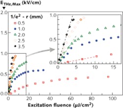
In conventional single photoconductive switches, high-voltage power supplies are needed to increase the terahertz emission. This problem is solved here by keeping the gap dimensions small such that typical values for the acceleration field on the order of several tens of kilovolts per centimeter are easily obtained with simple power supplies, while keeping the active area large.Performance of high-efficiency terahertz sources
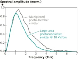
In combination with femtosecond laser sources, these two types of photoconductive antennas represent the central components of a powerful and easy-to-handle terahertz spectrometer. We compared the newly developed multiplexed photo-Dember emitters with a state-of-the-art, high-efficiency, large-area photoconductive emitter (see Fig. 3). Based on the amplitude of the Fourier spectra of both emitters, the multiplexed photo-Dember emitters are superior to the large-area photoconductive emitters biased with an accelerated electric field of 10 kV/cm. Surprisingly, the multiplexed photo-Dember emitter shows a broader spectrum and higher peak frequency than the large-area photoconductive emitter. The comparison of the two emitters was performed in our rapid-scanning terahertz precision spectrometer based on asynchronous optical sampling operating at 1 GHz repetition rate with an optical pulse energy limited to 1 nJ.3REFERENCES
1. G. Klatt et al., Opt. Exp. 18, 4939 (2010).
2. A. Dreyhaupt et al., Appl. Phys. Lett. 86, 121114 (2005).
3. G. Klatt et al., Opt. Exp. 17, 22847 (2009).
4. M. Beck et al., Opt. Exp. 18, 9251 (2010).
Thomas Dekorsy is a professor, Jure Demsar is an assistant professor, Stephan Winnerl is a researcher, and Matthias Beck and Gregor Klatt are Dipl. Phys. at Universität Konstanz, Postbox M 700, Universitätstraße 10, 78457 Konstanz, Germany; e-mail: [email protected]; www.uni-konstanz.de.


