INTERFEROMETERS: Interferometry helps optimize high-brightness LED production

DONG CHEN, ERIK NOVAK, and NELSON BLEWETT
The high-brightness light emitting diode (HB-LED) industry is experiencing rapid growth, with 2010 revenues expected to exceed 2009 revenues by more than 40%. The primary drivers for LED adoption include backlighting of LCD TVs and computer displays, automotive lighting, mobile phone and other handheld displays, and more efficient residential and commercial lighting. Each of these areas demands end products exhibiting tightly controlled efficiency and color, with center wavelength variation of no more than 4 nm, undetectable by the human eye. Optical interferometric profilometry has proven to measure and monitor HB-LED wafer surfaces rapidly and repeatably in 3D detail, enabling increased production efficiency and quality.
HB-LED design advances
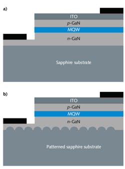
The structure of a typical LED consists of a stack of gallium nitride (GaN) layers epitaxially grown on a sapphire substrate (see Fig. 1). Usually only several percent of the total emitted light can be extracted due to the large difference in index of refraction between GaN materials and air. This causes total internal reflection at the device-air interface and light is lost back into the device. Several methods are used to enhance the light extraction efficiency, including random surface texturing, flip-chip technology, photonic crystal, and patterned sapphire substrates (PSS).
PSS structures have advantages for improving LED performance and are being widely used in HB-LED devices. To create the structures, only standard semiconductor photolithographic processes are required, which reduces the cost of implementation. In addition to enhancing light extraction efficiency, PSS structures reduce the dislocation defect density, both of which contribute to overall device efficiency. A high density of dislocation defects is often present in the GaN layer due to inherent large lattice mismatch and difference in thermal expansion coefficients in the epitaxial GaN layer.
Manufacturers utilize various PSS structure shapes to enhance LED performance and light extraction. The shape varies between manufacturers, with typical patterns including pyramidal, conical, or hemispherical shapes (see Fig. 2). Widths are generally several micrometers and heights are between 1 and 2 mm, with an overall pattern pitch between 2 and 5 mm. Most often shape is optimized in the development phase, while production manufacturers work to control the width, height, and pitch at a high sampling rate for process control. The height of these PSS structures is particularly crucial as deviations from the target value will affect efficiency, wavelength uniformity, and even create electrical shorts if the features penetrate the active layer. Also, as the deposition process is very slow, maintaining height uniformity can dramatically improve production throughput.3D surface metrology
Scanning electron microscopes are typically used to image PSS structures during the research phase and visualize fine details of the sidewall structure. Atomic force microscopes (AFMs) are also popular in research and for process control because they allow for nondestructive sample handling and high-resolution imaging; where sampling rates are such that throughput is not a factor, AFMs provide true 3D quantification of features, including subnanometer vertical resolution and very high slope capability. However, larger LED manufacturers process hundreds to thousands of PSS substrates daily and their throughput requires fast, accurate, nondestructive 3D surface metrology.
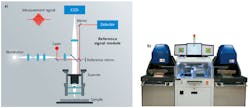
For rapid feedback on the production line, white-light interferometry (WLI) is becoming the technology of choice. White light interferometry, or optical interferometric profiling, has been used successfully in high-volume production environments for more than 25 years, providing areal 3D surface maps with nanometer-level accuracy and repeatability. These systems use a light beam from a broadband light source that is split in two by a beamsplitter (see Fig. 3). One beam reflects from a high-quality reference surface and the other reflects from the sample surface. The two beams are recombined at an optical detector, usually a CCD camera, and the difference in the paths that each follows produces a sinusoidal interference signal. The interference signal at the camera can be obtained only when the difference of the paths the two beams take is near zero. As the objective scans through focus in the vertical direction, each measured surface point will pass through this equal path location. When the paths are equal, the signal has maximum contrast. The vertical scan location of each maximum contrast point is noted for each pixel in the image; this maximum contrast map corresponds to a height map of the surface. The result is an accurate 3D surface characterization of the sample, much like topographic maps used by outdoor enthusiasts.For more measurement resolution and repeatability, the phase of the signal can be calculated and combined with the contrast map to create a final 3D height map of the object with subnanometer precision. In some systems, a separate laser interferometer provides a motion reference so that the system is self-calibrating rather than relying on a step standard for vertical accuracy. Continuous calibration enhances system stability in production.
Measurement optimization
Systems must be optimized to properly address the PSS application, as traditional interferometric optics and analysis techniques are unsuitable for gauge-capable production metrology. The main challenge is the high slope surface of the PSS conical features. The light collected by the microscope after reflection from the steep side slopes is weak, typically less than 5% of the signal from the flat portions of the substrate. The phase and location of the maximum contrast point calculated from this signal are quite noisy, which can lead to ambiguities in the height of the calculated surface.
The first step in improving the signal is to use an optimized microscope objective for imaging. Using a 115X, 0.8 NA objective, the signal from the steep slopes can be significantly improved versus using a standard 50X/0.55 NA or even a 100X/0.7 NA objective. The reference surface reflectivity can also be optimized to provide the best signal quality on these surfaces. Experiments show that for a low-signal location, the signal strength increases more than 2.5 times compared with the signal from a standard microscope objective. The reference surface reflectivity also can be optimized to provide the best signal quality on these surfaces. Maintaining focus in a standard production environment where temperature can fluctuate by a few degrees Celsius is also critical.
Even with the enhanced signal from improved optics, additional steps are needed to obtain accurate measurements. The good signal region is small and there is a high level of noise on the features. To improve results, the signal level for each pixel is mapped, and different processing is applied to regions of different signal levels. This produces a superior signal, which allows the height map from the phase to be accurately calculated across a broad area of PSS structures (see Fig. 4). With these techniques, standard deviation of height is less than 6 nm, 3 σ and less than 10 nm, 3 σ for width.Measurement at the production level
These enhancements can be implemented on systems with wafer handling for production measurements of PSS. Such systems have been deployed successfully for in-line process control. The 3 σ standard deviation of height, width, and pitch is less than 10 nm over a five-day period. Throughput of more than 60 wafers per hour for 2 in. substrates can be achieved with 13 sites measured on each wafer.
To achieve performance goals for efficiency and wavelength stability, HB-LED manufacturers use specialized structures to optimize output. The structures require stringent metrology to maintain wavelength stability, efficiency, and production throughput requirements. The measurement of these features is difficult to obtain due to their steep slopes and small sizes. Specialized optics can be used with white light interferometers to improve the signal strength; additional processing allows for gauge-capable, high-throughput results in production environments. These systems provide long-term 3 σ standard deviations of less than 10 nm on critical parameters of height, pitch, and width. This will result in higher quality and less expensive HB-LEDs.
Dong Chen is principal systems scientist, Erik Novak is director of technology development, and Nelson Blewett is a research applications engineer at Veeco Instruments, 2650 E. Elvira Rd., Tucson, AZ 85756; e-mail [email protected]; www.veeco.com.


