OPTICAL PROFILING: Modern optical surface profilers combine multiple techniques into a single, streamlined, user-friendly package
ROGER ARTIGAS
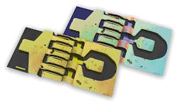
Photonics, materials science, and microtechnology are just a few of the many broad technological fields playing a progressively greater role in mainstream manufacturing. Complex microelectromechnical (MEMS) structures, for example, are now a regular feature of consumer electronics; ever more complex multilayer structures are used to enhance photovoltaic solar cell efficiency; and precision custom optics no longer have to be ground individually, but can instead be replicated much more rapidly as a complex aspheric.
Many of these high-tech applications increasingly make use of microstructures to achieve specific properties. Examples include diffraction effects to induce specific optical performance in optics, microfluidic anomalies for handling minute amounts of liquid materials, and surface enhancement effects for improving passivity or wear characteristics. At the finer end of the scale, application-specific micro- or even nanotexturing is rapidly becoming a sought-after attribute in medical, biophotonics, LEDs and organic LEDs, and many other technology fields.
As the complexity of these structures increases (and this at a variety of scales), so do the demands on manufacturing repeatability. And the tools needed to properly gauge the intended performance must also provide the requisite flexibility.
Optical profiling
As a helpful tool at the design stage and as a means of quality assessment during production, there is increasing demand for fast and powerful optical profiling systems that are also manufacturing-friendly. These systems ideally provide the capability to robustly measure rough, smooth, and stepped surface topologies and textures across a broad range of materials and complex structures.
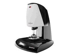
While several differing technologies are commercially available for completing this task, an increasing number of profiling systems make use of complementary optical techniques to optimize the flexibility of a single noncontact measurement system. At Sensofar, we originally pioneered the integration of multiple optical tools by combining optical confocal microscopy with corresponding interferometric techniques to enhance the versatility of optical profiling systems.
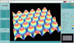
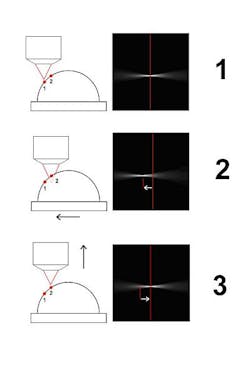
Phase-shift interferometry is a well-known optical profiling technology that provides exceptional sub-nanometer vertical resolution, even at low optical magnification. For smooth, continuous surfaces, it’s an ideal tool, but it fails on rough surfaces and steep slopes, as well as exhibiting ambiguity at surface discontinuities. White light interferometry takes up the baton for moderately rough surfaces, while a confocal measurement approach with a high-numerical-aperture (NA) objective is capable of measuring steep slopes as well as rough surfaces over a wide depth range. Modern high-end profiling systems use all of these techniques in varying guises to provide the greatest flexibility for measuring a broad range of surface forms and structures (see Fig. 1).
Complex optics
Application-specific lens designs are finding their way into a myriad of scientific and consumer applications. Microlenses form, for example, a vital component of portable microprojector designs, such as those available for home cinema. Fresnel lenses direct the light of high-power, white-light LEDs, leading to a very compact design with high light throughput and low power consumption. Special optics for biomedical applications improve imaging in endoscopes and in lab-on-a-chip devices used to compare tissue samples. Further examples include the optical couplers for VCSELs in telecommunications and the microlenses used for concentrating light into a microscopic waveguide (thus enabling the field of microoptoelectronic systems known as MOEMs).
Each of these applications, and many more, utilizes unique optical designs to address application-specific requirements. The production volume for any given application may run from the hundreds into the tens of thousands.
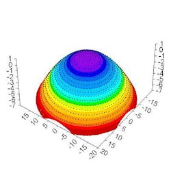
Take the case of complex aspherical optics. By straying from a true spherical shape, the spherical aberration can be reduced and specific optical performance can be achieved in a compact single lens. Additionally, by integrating diffractive effects into one surface of a lens, overall chromatic dispersion can be corrected (that is, reduced) to yield excellent color performance.
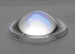
Standard spherical lenses can be cost-effectively “aspherized” using an optical polymer coating in a replication process. Alternatively, small or large numbers of lenses can be cost-effectively pressed from a mold (see Fig. 2). Complex, nonspherical optical designs and even diffractive structures can be diamond-turned directly into a mold. And while molded lenses cannot be expected to provide absolute high-end optical performance, a level of sophistication can be achieved that is normally only possible in traditional spherical optics through the use of doublet or more complex lens systems.Measurement multitalents
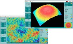
High-precision optical surfaces and the need for a more in-depth characterization of a lens or lens array require characterization using a combination of noncontact technologies. Correspondingly equipped, modern optical profiling systems can provide an integrated, complementary assessment of the surface profile and properties.
Typical high-end systems provide sub-nanometer resolution on all axes and usually comprise a feature set of the following:
- phase-shift and white light interferometry (PSI and WLI, respectively) to provide sub-nanometer vertical resolution over a wide area on smooth surfaces, or less accurate but more robust profile measurements for rougher surfaces, respectively;
- confocal metrology to give robust, high vertical and lateral resolution even on complex and steep surfaces, and utilizing modern microimaging techniques to aid and enrich the acquisition process;
- white light interferometry and spectral reflectometry to give vital information on thin-film makeup, ranging from sub-nanometer to 10 µm overall thickness and all at sub-nanometer resolution;
- twin CCDs, assigned to video and metrology tasks; and
- dual LEDs: blue for PSI and confocal measurements, and white for WLI and imaging tasks.
Outlook
Micro-optical measurement technology fulfills two important requirements of metrology: nondestructive measurement combined with high accuracy. By supplementing optical profiling systems with thin-film metrology capability, analysis algorithms, microdisplay technology in the optical path, and a compact sensor head, this technology can be configured very flexibly, ranging from a simple set-up for R&D and quality-inspection laboratories to the most complete and sophisticated arrangements for online process control.
Roger Artigas is vice president of optics at Sensofar Tech S.L., Terrassa, Spain; e-mail [email protected]; www.sensofar.com.
