PHOTOMULTIPLIER TUBES: Silicon photomultiplier technology goes fully digital
CARSTEN DEGENHARDT and HANS DRIESSEN
Silicon photomultipliers (SiPMs) have recently received a lot of interest as replacements for photomultiplier tubes (PMTs). Like PMTs, they are capable of measuring extremely low light levels, to the point of being able to detect single photons. However, when compared to PMTs, SiPMs offer the solid-state advantages of lower operating voltages, ruggedness, smaller physical size, lighter weight, and high immunity to magnetic fields.
Nevertheless, current SiPMs have limitations. Although they feature very high internal gain, they generate a relatively weak analog output signal that must be processed by a power-hungry readout application-specific integrated circuit (ASIC) to recover the photon count and the time of arrival of the first photon. The cost, size, and power consumption of this ASIC makes the transition from using conventional PMTs to SiPMs more difficult. A new all-digital SiPM technology developed at Philips eliminates the need for these external ASICs, opening up the viability of using solid-state devices in many more applications.
A different approach
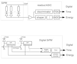
Although photon counting is by definition a digital task, conventional SiPMs combine the electrical pulses generated by multiple photon detections into a single analog output signal. As mentioned previously, this signal has to be processed by expensive power-consuming electronics to recover the photon count.
By integrating low-power CMOS electronics into the SiPM chip, we developed a digital SiPM in which each photon detected is converted directly into an ultrahigh-speed digital pulse that can be directly counted by on-chip counter circuitry. In contrast to conventional SiPMs, the digital SiPM is therefore an all-digital (digital-in/digital-out) device. As a result, it produces faster and more accurate photon counts with extremely well-defined timing of the first photon detection, both of which are important factors in applications such as medical-imaging scanners and high-energy nuclear-particle detectors. Moreover, the digital SiPMs can be fabricated using standard high-volume CMOS process technology.
Each microcell has its own ADC
Conventional SiPMs consist of a two-dimensional array of avalanche photodiodes (APDs), each of which is connected in series with its own polysilicon quenching resistor. All of these diode/resistor microcells are connected in parallel and the entire microcell array reverse-biased to a voltage above the diodes' normal breakdown voltage—typically in the range of 30 to 70 V. Operating in the so-called Geiger mode, the diodes are ultrasensitive to single electron-hole pairs that result in individual diodes experiencing avalanche breakdown. These electron-hole pairs can be generated either by the absorption of a photon (the desired signal), or by thermal energy or electron tunneling (unwanted background noise). The unwanted background noise produced by thermally generated electron-hole pairs and/or electron tunneling, together with false counts due to defective microcells, are collectively referred to as the SiPM's dark count.
To eliminate a conventional SiPM's need for an external digitizing ASIC, the digital SiPM developed by Philips equips each individual APD with its own one-bit on-chip analog-to-digital converter (ADC) in the form of a CMOS inverter (see Fig. 1). Each microcell that experiences avalanche breakdown therefore produces its own digital output that is captured, along with the digital outputs from all other triggered microcells, by an on-chip counter. Hence the digital SiPM converts digital events (photon detections) directly into a digital photon count. As a result, it is capable of achieving significantly better resolution than conventional SiPMs.
To overcome the dark-count problem associated with conventional SiPMs, each microcell in the digital SiPM is also equipped with an addressable static memory cell that can be used to disable or enable the microcell. Microcells that show high dark-count levels can thus be prevented from contributing false counts to the SiPM's output. This facility allows the digital SiPM to achieve better signal-to-noise ratios than conventional devices. Because defective microcells in the array can be disabled, it also helps to improve production yield.
Active quenching
Additional circuitry is added to each microcell to actively (rather than passively) quench and recharge the microcell after triggering. This active quenching/recharging in the device improves the detector's recovery time as well as reducing its power consumption. Detector modules constructed using the digital SiPMs typically only require air cooling. Cooling below ambient temperature is only required in applications that require ultralow dark-count levels.
In contrast to conventional analog SiPMs, in which parasitic capacitance and inductance degrade timing performance, all microcells in the digital SiPM are connected via a low-skew balanced trigger network to an on-chip time-to-digital converter. The timing resolution of this converter is 20 ps, preserving the excellent intrinsic timing performance of the Geiger-mode APDs.
In implementing this new digital SiPM technology, the challenge was to integrate the relatively high-voltage APDs, which must be reverse-biased to around 30 V, alongside low-voltage CMOS logic on the same silicon chip, while maintaining dark count and photon-sensitivity performance.
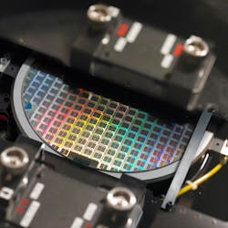
We have achieved a fully integrated 64 pixel sensor with a sensing surface of greater than 10 cm2 and a power consumption less than 15 mW/cm2, using 180 nm CMOS technology on 8 in. wafers (see Fig. 2). The device's photon-detection efficiency is 30% at 450 nm; it has an optical crosstalk of 8% and a dark-count rate of 100 kHz/mm2 at 20°C and 900 Hz/mm2 at -40°C.Applications
The planar nature of the digital SiPMs allows them to be closely coupled to suitable scintillator materials for the detection of nuclear particles and high-energy electromagnetic radiation. When struck by an incoming particle or high energy electromagnetic radiation, scintillator materials absorb the energy and re-emit it in the form of a weak flash of light, typically in the visible spectrum. This flash is then detected by the photomultiplier. Digital SiPMs are thus suited for use in particle physics experiments and medical-imaging equipment—for example, in positron-emission tomography (PET) scanners.
Positron-emission tomography is a molecular-imaging technique that produces three-dimensional images of functional processes in the body—for example of the uptake of glucose that fuels metabolic activity. The PET system detects pairs of gamma rays originating from a radioactive tracer, a small amount of which is injected into the patient prior to the scan. To image metabolic activity, PET typically uses a radioactive derivative of glucose called fluorodeoxyglucose (FDG). This compound mimics the behavior of glucose in the body and can be detected by the PET system.
For so-called time-of-flight PET scanners, accurately determining the time at which the first photon arrives at the detector is extremely important. The digital SiPM prototypes achieve a timing accuracy for the detection of the first photon of around 190 ps full-width, half-maximum using a standard lutetium yttrium orthosilicate scintillator crystal at 511 keV for two detectors in coincidence.
Other applications for digital SiPMs include fluorescence-based DNA sequencing, protein/DNA microarray assays, surveillance systems, and night-vision systems.
Carsten Degenhardt is project manager and Hans Driessen is senior communications manager at Philips Digital Photon Counting, Eindhoven, the Netherlands; e-mail: [email protected]; www.philips.com.

