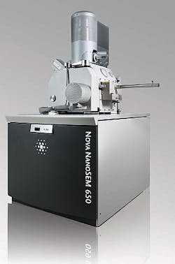
Electron microscopes from FEI offer beam deceleration
The Nova NanoSEM 50 Series of ultrahigh-resolution scanning electron microscopes can examine highly insulating samples in low vacuum with little or no preparation. It has beam deceleration and low vacuum capabilities, a universal large chamber, and a 16 bit scan engine. It includes a new suite of retractable and in-lens detectors.
FEI
Hillsboro, OR
http://fei.com/nova-nanosem-50
-----
PRESS RELEASE
FEI Introduces Nova NanoSEM 50 Series
New family of electron microscopes combines ultra-high resolution and analytical performance for the widest range of materials
Hillsboro, Ore./August 2, 2010―FEI Company (NASDAQ: FEIC), a leading scientific instrumentation company providing electron microscope systems for nanoscale applications across many industries, announced today the availability of its new Nova™ NanoSEM 50 Series of ultra-high resolution scanning electron microscopes (UHR SEMs). It is designed to provide industry-leading, nanometer-scale resolution and ultra-precise analysis on the widest range of samples. Initial shipments are planned for the fourth quarter of this year.
“This newest generation of the well-established Nova NanoSEM offers a unique combination of capabilities unequalled by any other UHR SEM,” said George Scholes, FEI’s Research Division vice president and general manager. “In one instrument, you get imaging down to the nanometer level, high beam current for fast and precise analysis, and low vacuum capability to extend the range of sample types and minimize preparation requirements. Customers no longer have to choose between ultra-high resolution (at high and low kV) and analytical performance. The Nova NanoSEM makes no compromise—it delivers both in one system.”
In low vacuum, the Nova NanoSEM can examine highly insulating samples, up to nearly the same resolution that can be achieved in high vacuum, with little or no preparation, eliminating artifacts and saving time.
The Nova NanoSEM 50 Series builds on the success of previous Nova NanoSEM instruments, and adds technological innovations from FEI’s other industry-leading product families:
- It inherits its proven beam deceleration and low vacuum capabilities (including the Helix detector for unequalled high-contrast, low-noise imaging) from previous-generation Nova NanoSEMs.
- Its integrated sample & chamber cleaning solutions, critical for low kV high-resolution imaging, and its advanced and intuitive sample navigation and user interface, debuted on the Quanta™ and Magellan™ SEMs.
- And its universal large chamber, 16-bit scan engine and latest scanning strategies, as well as the high-precision stage, were first deployed in the Nova and Helios™ NanoLab DualBeam™ systems.
- The Nova NanoSEM 50 Series introduces a new suite of detectors, retractable and in-lens, for optimized secondary electron (SE), backscattered electron (BSE), and scanning transmission electron microscopy (STEM) signal collection and filtering.
The Nova NanoSEM 450 is ideally suited for advanced material science applications. Its 110 mm stage with up to 75-degree motorized tilt accepts a wide range of sample sizes and configurations, and permits electron back-scattered diffraction (EBSD) analysis without pre-tilted holders.
The Nova NanoSEM 650 offers a high-precision 150 mm piezo-electric stage for fast, precise navigation, providing 100-percent coverage of six-inch wafers or masks, and substatial coverage of eight-inch samples. Fast beam blanking, integrated 16-bit pattern generator, and a variety of beam chemistries for e-beam deposition make it ideal for prototyping and lithography applications. Both instruments provide 1 nm resolution at 15 kV, 1.4 nm at 1 kV, and beam currents up to 200 nA.
For more information, please visit http://fei.com/nova-nanosem-50
About FEI
FEI (Nasdaq: FEIC) is a leading diversified scientific instruments company. It is a premier provider of electron and ion-beam microscopes and tools for nanoscale applications across many industries: industrial and academic materials research, life sciences, semiconductors, data storage, natural resources and more. With a 60-year history of technological innovation and leadership, FEI has set the performance standard in transmission electron microscopes (TEM), scanning electron microscopes (SEM) and DualBeams™, which combine a SEM with a focused ion beam (FIB). FEI’s imaging systems provide 3D characterization, analysis and modification/prototyping with resolutions down to the sub-Ångström (one-tenth of a nanometer) level. FEI’s NanoPorts in North America, Europe and Asia provide centers of technical excellence where its world-class community of customers and specialists collaborate. FEI has approximately 1800 employees and sales and service operations in more than 50 countries around the world. More information can be found at: www.fei.com <http://www.fei.com/> .
-----
Posted by Lee Mather
Follow OptoIQ on your iPhone; download the free app here.
Subscribe now to Laser Focus World magazine; it's free!
