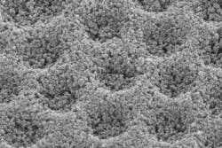
Thin, potentially flexible dye-sensitized solar cell relies on plasmonic nanodomes
Palo Alto--A group of engineers at Stanford University are integrating plasmonics into solar cells to improve their performance and make them more lightweight.1 One advantage of photovoltaic (PV) cells based on plasmonics: the active layer can be much thinner, bringing electrons closer to the electrodes.
The researchers created a hexagonal array of metallic nanodimples, with each dimple a few nanometers in size, using a template to form the dimples in a layer of titania on a transparent substrate. The arrays were then layered with a photosensitive dye and a film of silver, filling the dimples. From the direction of the transparent substrate, the features appear as an array of nanodomes.
Photons that interact with the cell to form electric current are either directly absorbed by the dye or turned into plasmons when they hit the nanodomes. Because the cell itself is thin and easily printable, it could potentially be fabricated on cloth or other flexible roll-up substrates.
The cell is not very efficient at present, but the researchers believe they could eventually boost efficiency to 15%—a very high figure for dye-sensitized solar cells.
REFERENCE:
1. I-Kang Ding et al., Advanced Energy Materials, Vol. 1, Issue 1, p. 52 (2011).
Subscribe now to Laser Focus World magazine; it’s free!

John Wallace | Senior Technical Editor (1998-2022)
John Wallace was with Laser Focus World for nearly 25 years, retiring in late June 2022. He obtained a bachelor's degree in mechanical engineering and physics at Rutgers University and a master's in optical engineering at the University of Rochester. Before becoming an editor, John worked as an engineer at RCA, Exxon, Eastman Kodak, and GCA Corporation.
