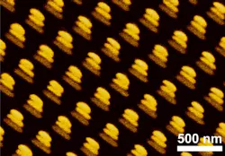
Nano TV antennas could improve optical data transfer, LEDs, photodetectors
Stuttgart, Germany--In collaboration with researchers at the Max-Planck-Institute for Solid State Research, physicists at the University of Stuttgart have created metallic antennas 100 nm in size that efficiently receive optical frequencies in the range of several hundreds of terahertz (the 1500 nm wavelength near-IR optical-communications region).1 Such nanoantennas could speed up optical data transfer.
Standard TV antennas receive signals carried by electromagnetic waves with frequencies in the megahertz regime and convert them into pulses of electric current in connected cables. The antenna connects two very different length scales: the carrier wavelength, ranging from centimeters to meters, and the size of the wiring, typically on the millimeter scale. The German research group has applied this radio-frequency antenna concept to the optical wavelength regime.
Nano-sized Yagi-Uda antennas
Certain antenna geometries are known to receive radiation from designated directions. Such a unidirectional TV-antenna is the so-called Yagi-Uda antenna, invented in Japan by Yagi and Uda in 1926. Consisting of several aligned parallel dipole antennas of different lengths, the Yagi-Uda antenna can be tuned to receive signals from a given direction five to ten times more efficiently than a dipole antenna. The received signal can be even more enhanced by several orders of magnitude when the single antenna is expanded to an array of Yagi-Uda antennas. Such antenna arrays are used to transmit signals over very large distances, for example in satellite communications.
(Note: Back in 2010, researchers from Hiroshima University (Higashihiroshima, Japan) also created nano-sized Yagi-Uda antennas for use at optical frequencies. Their antennas were used for emitting light rather than receiving it.)
The German Yagi-Uda antennas are made of 3D gold wire arrays of different lengths stacked in layers with dielectric material in between. A periodic arrangement of single Yagi-Uda nanoantennas form the optical antenna arrays.
Coupling to normal-incidence radiation
Measurements on the 3D arrays show that the amount of absorbed energy strongly depends on the angle of incidence and on the frequency of the incident electromagnetic waves. The scientists showed in particular that maximal absorption of incident radiation occurs at 200 THz, only if light impinges from the direction parallel to the antenna axis of the individual Yagi-Uda antenna. For this particular situation, the incoming wave of 1500 nm length is confined to a subwavelength region only about 100 nm in size. This phenomenon could be used in the future for very sensitive detection of near-IR radiation on the nanoscale.
One of the big advantages of the optical antenna array is the fact that its 3D character couples to radiation normal to the surface. This is advantageous for light emitters, such as LEDs, or very sensitive photodetectors. Furthermore, the researchers showed in numerical calculations that a phased-array beam steerer could be created.
REFERENCE:
1. Daniel Dregely et al., Nature Communications 2, doi:10.1038/ncomms1268, published 05 April 2011.
About the Author
John Wallace
Senior Technical Editor (1998-2022)
John Wallace was with Laser Focus World for nearly 25 years, retiring in late June 2022. He obtained a bachelor's degree in mechanical engineering and physics at Rutgers University and a master's in optical engineering at the University of Rochester. Before becoming an editor, John worked as an engineer at RCA, Exxon, Eastman Kodak, and GCA Corporation.

