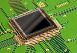
SeeBetter to develop advanced silicon retina for artificial vision
Leuven, Belgium--A new European project called SeeBetter, launched earlier this year, has the goal of designing and building a high-performance silicon retina using advanced photodetector and packaging technology. The new sensors have the potential to benefit artificial vision and find wide application in industry. (Here, "silicon retina" refers to a photodetector array with some retinal properties, and not an intraocular implant.)
Neuromorphic sensor
Conventional image sensors are fundamentally limited by comparison with biological retinas, because they produce redundant sequences of images at a limited frame rate. By contrast, neuromorphic "silicon retina" vision sensors mimic the biological retina's information processing capability by computing the salient spatial and temporal aspects of the visual input and encoding this information in a frame-free data-driven asynchronous spiking output.
The range of applications of these silicon retinas remain restricted because of their low quantum efficiency and their inability to combine high-quality spatial and temporal processing on the same chip. Solutions to these technical challenges would revolutionize artificial vision by providing fast, low-power sensors with biology's superior local gain control and spatiotemporal processing. Such sensors would find immediate and wide applications in industry, and provide technology for future vision prostheses.
Multidisciplinary effort
SeeBetter aims at addressing these limitations by realizing an advanced silicon retina with the superior quantum efficiency and spatiotemporal processing of biological retinas. Seebetter will build on multidisciplinary expertise in biology, biophysics, biomedical, electrical, and semiconductor engineering.
Objectives of the project are:
--to better understand the functional roles of the six major classes of retinal ganglion cells using genetic and physiological techniques
--to use this understanding to mathematically and computationally model retinal vision processing from the viewpoint of biology, machine vision, and future retinal prosthetics
--to design and build the first high-performance silicon retina with a heterogeneous array of pixels specialized for both spatial and temporal visual processing
--to combine this silicon retina with an optimized photodetector wafer with high quantum efficiency using state-of-the-art backside illumination and hybridization technologies.
Imec is coordinating this project as well as contributing its image sensor and hybridization technologies. Imec will take care of the design of the photodetector in the imaging system. The fabrication of the photodetector and its hybridization to the CMOS electronics will be done using Imec's 200 mm fabrication line.
SeeBetter is a 'small or medium-scale focused research project (STREP)' project (number 270324) in FET proactive ICT Call 6 (FP7-ICT-2009-6) in the work program Brain-inspired ICT. The members of the SeeBetter consortium are the Friedrich Miescher Institute for Biomedical Research (Switzerland), Imec (Belgium), Imperial College London (United Kingdom) and the University of Zurich (Switzerland).
For more information, visit www.seebetter.be.
Subscribe now to Laser Focus World magazine; it’s free!

John Wallace | Senior Technical Editor (1998-2022)
John Wallace was with Laser Focus World for nearly 25 years, retiring in late June 2022. He obtained a bachelor's degree in mechanical engineering and physics at Rutgers University and a master's in optical engineering at the University of Rochester. Before becoming an editor, John worked as an engineer at RCA, Exxon, Eastman Kodak, and GCA Corporation.
