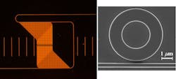
Microspectrometer has donut instead of ring resonators for higher resolution
Atlanta, GA--An 81-channel microspectrometer with 2-micron-diameter single-mode microdonut resonators as its sensing elements is vastly shrunken in size compared to conventional spectrometers, but without sacrificing resolution.1 Fabricated on a silicon-on-insulator chip, the instrument was developed at the Georgia Institute of Technology for integrated lab-on-a-chip sensing applications.
Tunable-laser light in the 1550 nm range from an input-bus waveguide enters the microdonut array, with each microdonut resonator tapping only a small portion of the incoming light; each resonator is a unique channel and has a slightly different diameter. In a microdonut resonator, the fundamental radial mode interacts only with the donut's outer wall; this is in contrast to a more-conventional microring resonator, in which the light interacts with the inner and outer walls. Less interaction means a higher quality (Q) factor; the microdonuts have a loaded Q of 30,000 and an intrinsic Q of 80,000. The signal is collected by imaging from the top of the chip
The device achieved 0.6 nm resolution over a spectral range of more than 50 nm with a footprint less than one square millimeter. The simple instrument can be integrated with other devices, including sensors, optoelectronics, microelectronics, and microfluidic channels for use in biological, chemical, medical, and pharmaceutical applications.
The group, led by Ali Adibi, is currently developing the next generation of these spectrometers, which are being designed to contain up to 1000 resonators and achieve 0.15 nm resolution with a spectral range of 150 nm.
The research was supported by the Air Force Office of Scientific Research and the Defense Advanced Research Projects Agency.
REFERENCES:
1. Zhixuan Xia et al., Optics Express, Vol. 19, No. 13, p. 2356 (2011); doi:10.1364/OE.19.012356.
Subscribe now to Laser Focus World magazine; it's free!

John Wallace | Senior Technical Editor (1998-2022)
John Wallace was with Laser Focus World for nearly 25 years, retiring in late June 2022. He obtained a bachelor's degree in mechanical engineering and physics at Rutgers University and a master's in optical engineering at the University of Rochester. Before becoming an editor, John worked as an engineer at RCA, Exxon, Eastman Kodak, and GCA Corporation.
