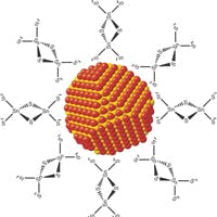
Quantum-dot ink could be low-cost semiconductor layer for photovoltaics
Argonne, IL--Inorganic nanocrystal arrays fabricated from a quantum-dot "ink" can serve as potentially lower-cost semiconductor layers for solar cells.1 The ink was developed by researchers at the University of Chicago and the U.S. Department of Energy's Argonne National Laboratory.
The nanocrystal arrays have excellent electron mobility and could be a step towards addressing fundamental problems with current solar technology. One way to make photovoltaic cells more economically than standard sliced crystalline silicon cells would be to print them. "You'd use a kind of ink, stamped on using a roll technology with a flexible substrate," said team leader Dmitri Talapin.
Creating a photovoltaic ink, however, requires a precursor that is soluble. The team developed that precursor using quantum dots held in a matrix by molecular metal chalcogenide complexes. The process heats the material to about 200°C, resulting in a layer of material with good semiconducting properties.
"The electron mobility for this material is an order of magnitude higher than previously reported for any solution-based method," Talapin said.
REFERENCE:
1. Jong-Soo Lee et al., Nature Nanotechnology (2011); doi:10.1038/nnano.2011.46, Published online 24 April 2011.
Subscribe now to Laser Focus World magazine; it's free!

John Wallace | Senior Technical Editor (1998-2022)
John Wallace was with Laser Focus World for nearly 25 years, retiring in late June 2022. He obtained a bachelor's degree in mechanical engineering and physics at Rutgers University and a master's in optical engineering at the University of Rochester. Before becoming an editor, John worked as an engineer at RCA, Exxon, Eastman Kodak, and GCA Corporation.
