PLASMONICS: Surface-plasmon resonance imaging just got easier
The ability to image surface-plasmon resonances allows researchers to map the local electric fields that create the unusual optoelectronic properties of metamaterials, for example. But although such imaging is possible beyond the diffraction limit, costly cathodoluminescence and electron-energy-loss spectroscopy techniques can only be used in a vacuum, while scanning near-field optical microscopy is also costly, has a long scanning time, and requires a very complex setup to achieve even 50 nm resolution.
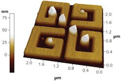
An alternative imaging method from researchers at Katholieke Universiteit Leuven (Leuven, Belgium) and collaborators builds on the discovery that illumination of nanostructures with light from a Ti:sapphire laser (800 nm, 0.98 mW) produces local field enhancements in “hotspot” regions where surface plasmons are generated. These regions can then be observed using a standard confocal or second-harmonic-generation microscope. But when the illumination is removed, further analysis of the nanostructures (fabricated in nickel and palladium) shows a permanent physical imprint of these plasmonic patterns on the nanostructures.
Analysis shows that these imprinted patterns or “hotspot decorations” are actually composed of small amounts of the metals from which the nanostructures were fabricated and directly coincide with the local-field-enhancement locations. These structures are easily imaged with resolution values dictated by the scanning-probe technique used for analysis.

John Wallace | Senior Technical Editor (1998-2022)
John Wallace was with Laser Focus World for nearly 25 years, retiring in late June 2022. He obtained a bachelor's degree in mechanical engineering and physics at Rutgers University and a master's in optical engineering at the University of Rochester. Before becoming an editor, John worked as an engineer at RCA, Exxon, Eastman Kodak, and GCA Corporation.
