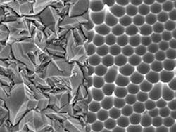
Nanomold creates better antireflection coating for silicon photovoltaics
Lausanne, Switzerland--To improve the absorption of silicon photovoltaic (PV) cells, scientists at the Swiss Federal Institute of Technology in Lausanne (EPFL) have created a new way to fabricate a zinc oxide (ZnO) antireflection coating.1 The approach eliminates the inherent random nature of ZnO nanopyramidal coatings by molding the pyramids rather than growing them by crystallization.
One of the costs of making silicon PV cells is the silicon itself: silicon boules are grown and then wafers are sliced from the boules. If the wafers can be made thinner, they cost less. But thinner wafers trap less light; adding a ZnO pyramidal scattering layer aids the trapping.
But scientists are attempting to beat the performance of naturally grown ZnO crystals. “It is difficult to modify the natural pyramidal shape of these crystals in order to obtain even better light scattering,” says researcher Corsin Battaglia, “so we had the idea to force the crystals to grow on a different support, an inverted mold with the desired structure.”
Once the thin layer of ZnO is deposited on the mold all that needs to be done is to “demold” it to obtain a film with the desired structure. This procedure, described in the September edition of the journal Nature Photonics, not only increases the amount of light that is trapped, thereby increasing output, but also has the potential to reduce the cost of the cells because of its compatibility with mass production.
REFERENCE:
1. Corsin Battaglia et al., Nature Photonics online (2011). doi: 10.1038/NPHOTON.2011.198

John Wallace | Senior Technical Editor (1998-2022)
John Wallace was with Laser Focus World for nearly 25 years, retiring in late June 2022. He obtained a bachelor's degree in mechanical engineering and physics at Rutgers University and a master's in optical engineering at the University of Rochester. Before becoming an editor, John worked as an engineer at RCA, Exxon, Eastman Kodak, and GCA Corporation.
