Optically driven nanomechanical resonators could become nonvolatile memory devices
(Image: Yale University)
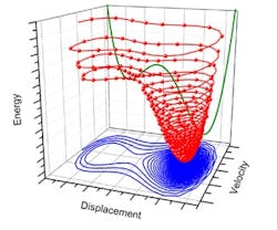
New Haven, CT--Nanoscale optomechanical resonators developed by engineers at the Yale School of Engineering and Applied Science operate at much higher amplitudes than previously thought.1 The slightly buckled resonators, cooled to their quantum ground states (an achievement in itself), take one of two stable buckled configurations; the coupling to an optical cavity generates enough phonons (mechanical waves akin to sound waves) to overcome the energy barrier and flip the resonators to their other state.
Such manipulations allow the Yale researchers to observe evidence for theoretical predictions, such as nanomechanical "slow-downs" and a zero-frequency singularity (oddity). Able to be flipped from one state to the other, the device also has potential to serve as a nonvolatile nano-optomechanical memory. Oscillation amplitudes are in the hundreds of nanometers, and frequencies are in the megahertz range.
The operating principle is similar to laser cooling techniques used in atomic physics. “One can control the motion of a mechanical structure, amplify or cool its vibrations, just by controlling the wavelength of laser light,” said Mahmood Bagheri, one of the researchers.
Among other benefits, optomechanical memory devices can withstand harsher environments than electronic or magnetic memory devices without losing data. Future technologies containing similar high-amplitude optomechanical resonators might be less sensitive to environmental conditions, such as variations in temperature and radiation. At the same time, high-amplitude resonators might enable more accurate and robust measuring devices.
REFERENCE:
1. Mahmood Bagheri et al., Nature Nanotechnology (2011); published online 23 October 2011; doi:10.1038/nnano.2011.180.
