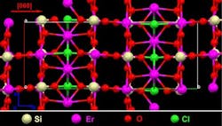
Erbium chloride silicate, a new photonic material, can enhance energy, computer, lighting technologies
Phoenix, AZ--A new erbium (Er) compound created at Arizona State University and called erbium chloride silicate (ECS) contains Er as an integral part of the structure rather than as a dopant.1 The researchers fabricated it in the form of a silicon-ECS single-crystal core-shell nanowire.
Because the density of Er atoms (1.6 x 1022 cm-3) in ECS is a factor of 1000 greater than the maximum amount that can be introduced in Er-doped materials, ECS greatly increases Er's optical activity (such as high-gain light emission) in a silicon-compatible material. In addition, because the Er atoms are organized in a periodic array, they do not cluster in this new compound, resulting in higher optical quality.
Cun-Zheng Ning, one of the researchers, says that with the high Er concentration, many devices can be integrated into a chip-scale system. “Thus the new compound materials containing erbium can be integrated with silicon to combine computing and communication functionalities on the same inexpensive silicon platform to increase the speed of computing and Internet operation at the same time," he explains.
Erbium materials can also be used to increase the energy-conversion efficiency of silicon photovoltaic (PV) cells. Silicon does not absorb solar radiation with wavelengths longer than 1.1 microns, which results in a waste of energy. But Er can convert two or more IR photons to one visible photon, which is absorbed by the cell. Erbium can also downconvert UV photons into the visible, making two from one—valuable not just for silicon PV cells but for white-light LEDs as well.
Like many scientific discoveries, the synthesis of ECS came about somewhat by accident. “Similar to what other researchers are doing, we were originally trying to dope Er into silicon nanowires. But the characteristics demonstrated by the material surprised us,” he says. “We got a new material. We did not know what it was, and there was no published document that described it. It took us more than a year to finally realize we got a new single-crystal material no one else had produced.”
Ning and his team are now trying to use ECS for increasing silicon PV-cell efficiency and making miniaturized optical amplifiers for chip-scale photonic systems.
“Most importantly,” he says, “there are many things we have yet to learn about what can be achieved with use of the material. Our preliminary studies of its characteristics show it has many amazing properties and superior optical quality.”
REFERENCE:
1. Anlian Pan et al., Optical Materials Express, Vol. 1, Issue 7, p. 1202 (2011) http://dx.doi.org/10.1364/OME.1.001202.
About the Author
John Wallace
Senior Technical Editor (1998-2022)
John Wallace was with Laser Focus World for nearly 25 years, retiring in late June 2022. He obtained a bachelor's degree in mechanical engineering and physics at Rutgers University and a master's in optical engineering at the University of Rochester. Before becoming an editor, John worked as an engineer at RCA, Exxon, Eastman Kodak, and GCA Corporation.

