Inkjet-printed carbon-nanotube electronics may lower manufacturing costs for OLED displays
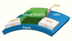
Los Angeles, CA--Researchers from Aneeve Nanotechnologies, a startup company working from the University of California, Los Angeles (UCLA) on-campus technology incubator at the California NanoSystems Institute (CNSI), have created thin-film transistor circuits based on single-walled carbon nanotubes for organic LED (OLED) displays.1 The potentially low-cost fabrication process lends itself to roll-to-roll printing—a significant step, as much effort is being expended to develop roll-to-roll manufactured OLEDs on flexible plastic or metal substrates.
The researchers solved many material integration problems, developed new cleaning processes, and created new methods for negotiating nano-based ink solutions. They made carbon-nanotube thin-film transistors with high mobility and a high on-off ratio, completely based on ink-jet printing, demonstrating the first fully printed single-pixel OLED control circuits. The fully printed thin-film circuits showed significant performance advantages over traditional organic-based printed electronics.
The startup includes collaborators from the departments of materials science and electrical engineering at the UCLA Henry Samueli School of Engineering and Applied Science and the department of electrical engineering at the University of Southern California.
"We have demonstrated carbon nanotubes' viable candidacy as a competing technology alongside amorphous silicon and metal-oxide semiconductor solution as a low-cost and scalable backplane option," said Kos Galatsis, a co-founder of Aneeve.
For active-matrix OLED applications, the printed carbon nanotube transistors will be fully integrated with OLED arrays, the researchers said. The encapsulation technology developed for OLEDs will also keep the carbon nanotube transistors well protected, as the organics in OLEDs are very sensitive to oxygen and moisture.
The technology incubator at the CNSI was established two years ago to nurture early-stage research and to help speed the commercial translation of technologies developed at UCLA. Aneeve Nanotechnologies LLC has been conducting proof-of-concept work at the tech incubator with the mission of developing low-cost, high-performance electronics using nanotechnology to bridge the gap between emerging and traditional platforms.
REFERENCE:
1. Pochiang Chen et al., Nano Letters, publication date (Web): November 3, 2011; DOI: 10.1021/nl202765b

John Wallace | Senior Technical Editor (1998-2022)
John Wallace was with Laser Focus World for nearly 25 years, retiring in late June 2022. He obtained a bachelor's degree in mechanical engineering and physics at Rutgers University and a master's in optical engineering at the University of Rochester. Before becoming an editor, John worked as an engineer at RCA, Exxon, Eastman Kodak, and GCA Corporation.
