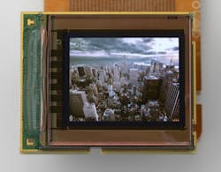
MicroOLED unveils highest-pixel-density OLED microdisplay
Grenoble, France--MicroOLED has introduced a low-power OLED (organic light-emitting diode) with 5.4 million pixels and a 0.61 in. diagonal. The display is intended for demanding applications such as professional camera and camcorder equipment, night-vision systems, and head-mounted displays used in surgery.
The display's sub-pixel pitch of 4.7 by 4.7 micrometers is the highest pixel density OLED microdisplay available, says MicroOLED. The company eliminated the black matrix gap between pixels increasing the proportional illuminated area while decreasing pixel size. The OLED display has a maximum 100,000:1 contrast and a 96% uniformity, and can operate on as little as 0.2 W of electrical power even when the fully digital video input is embedded.
MicroOLED will market the 5.4 million-pixel density 0.61 inch diagonal microdisplay to address needs in three areas: head-mounted displays used by surgeons, where high resolution and quality of colors and contrast are a must; professional cameras and camcorders; and night vision applications, where heightened contrast and uniformity enable defense and security engineers to improve the performance of detection and identification equipment.
The 5.4 million-pixel density microdisplay comes in full color (16 million color) SXGA or monochrome formats (2,560 by 2,048 pixels), both with digital video input.
Founded in 2007, MicroOLED is a privately held company led by a management team with several years’ research and development experience in OLED technology from CEA-LETI, the European micro-and nanotechnology research center.

John Wallace | Senior Technical Editor (1998-2022)
John Wallace was with Laser Focus World for nearly 25 years, retiring in late June 2022. He obtained a bachelor's degree in mechanical engineering and physics at Rutgers University and a master's in optical engineering at the University of Rochester. Before becoming an editor, John worked as an engineer at RCA, Exxon, Eastman Kodak, and GCA Corporation.
