In theory, surface-plasmon-driven superlens looks promising for wideband use
Houghton, MI--Durdu Güney, an assistant professor of electrical and computer engineering at Michigan Technological University, has taken a step toward creating a superlens that could use visible light to see objects as small as 100 nm across.1 The lens would be made of an optical plasmonic metamaterial.
Other researchers have been able to create superlenses that sidestep the diffraction limit, but not throughout the entire visible spectrum. Güney’s model shows how metamaterials might be “stretched” to refract light from the IR through the visible and into the UV.
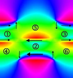
In the superlens, a thin metal film interacts with a periodic array of nanostructures around it, resulting in a surface-plasmon-driven metamaterial with a double negative refractive index (simultaneous negative permittivity and permeability). Making these superlenses could be relatively inexpensive, possibly even enabling them to find their way into cell phones. But there would be other uses as well, says Güney.
“It could also be applied to lithography," he says. Semiconductor-chip patterns are made using light from UV excimer lasers. “With this superlens," says Güney, "you could use a red laser, like the pointers everyone uses, and have simple, cheap [optical lithography] machines, just by changing the lens.”
What excites Güney the most, however, is that a cheap, accessible superlens could open our collective eyes to worlds previously known only to a very few. “The public’s access to high-powered microscopes is negligible,” he says. “With superlenses, everybody could be a scientist. People could put their cells on Facebook. It might just inspire society’s scientific soul.”
REFERENCE:
1. Muhammad I. Aslam and Durdu Ö. Güney, Physical Review B 84, 195465 (2011); DOI: 10.1103/PhysRevB.84.195465

John Wallace | Senior Technical Editor (1998-2022)
John Wallace was with Laser Focus World for nearly 25 years, retiring in late June 2022. He obtained a bachelor's degree in mechanical engineering and physics at Rutgers University and a master's in optical engineering at the University of Rochester. Before becoming an editor, John worked as an engineer at RCA, Exxon, Eastman Kodak, and GCA Corporation.
