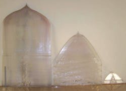
Wright-Patterson Air Force Base, OH--Researchers at the Air Force Research Laboratory (AFRL) and Saint-Gobain Ceramics and Plastics have figured out a way to make larger and thicker sapphire windows for electro-optics and IR optical systems. The new manufacturing process results in sapphire windows up to 16 in.wide by 18 in. long and 0.8 in. thick. The process meets all transmission and durability requirements while reducing postproduction costs, according to the AFRL.
There are only a limited number of crystal-growth techniques able to produce single-crystal sapphire suitable for window applications larger than 6 in., and only a few of them are capable of producing commercially available plates in larger sizes that are suitable for fabrication into a finished window. In response, the AFRL and Saint-Gobain extended the state of the art of edge-defined film-fed growth (EFG) for growing near-net-shape sapphire. They conducted design experiments, thermal modeling, and experimental growth trials. The new size capability enables fabrication of the sapphire sheets required by the Navy's DDG 1000 (Zumwatt-class destroyer) program. The manufacturing process is also under evaluation by the Air Force's Cobra Ball aircraft and by the Army's High Mobility Artillery Rocket System Office.
Demand for large-area windows for EO and IR applications in the visible to mid-wave IR has increased considerably in the last 10 years: applications in both the military and civilian arenas, such as sensing and other optics for aircraft, missiles, and ships, require hard, strong, and transparent materials to achieve system goals. With a Mohs hardness of 9.0 and a wide transmission window in the visible and IR, sapphire has properties that are suitable for extremely demanding uses.
Source: www.wpafb.mil/news/story.asp?id=123286091

John Wallace | Senior Technical Editor (1998-2022)
John Wallace was with Laser Focus World for nearly 25 years, retiring in late June 2022. He obtained a bachelor's degree in mechanical engineering and physics at Rutgers University and a master's in optical engineering at the University of Rochester. Before becoming an editor, John worked as an engineer at RCA, Exxon, Eastman Kodak, and GCA Corporation.
