MIT sawtooth-shaped broadband metamaterial design could boost PV cell efficiency
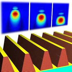
Cambridge, MA--An optical metamaterial conceived by scientists at the Massachusetts Institute of technology (MIT), along with their international colleagues, is made of periodic sawtooth-shaped ridges that, because they slope, absorb different wavelengths of IR light at different heights, resulting in high-efficiency broadband absorption.1 Possible uses include high-efficiency photovoltaic (PV) cells and tailored-wavelength IR detectors.
At present, the metamaterial is only a design, but the MIT group is pursuing experimental verification. The MIT researchers collaborated with researchers at Zhejiang University and Taiyuan University in China, and the University of Illinois at Urbana-Champaign in designing the metamaterial.
Slow-light device
The structure consists of alternating planar layers of metal and dielectric stacked and etched to form the tapered ridges. The absorptivity at normal incidence is 95% over a wide range of IR wavelengths, and remains high over a wide range of incidence angles. The longer wavelengths are trapped toward the bottoms of the sawteeth, while shorter wavelengths are trapped higher up on the teeth. The anisotropic metamaterial is actually a "slow-light" device.
The metamaterial can be fabricated using standard PV-manufacturing equipment, say the researchers. Nicholas Fang, a professor in MIT's mechanical-engineering department, notes that, because the material is efficient at emission as well as absorption, it could also be used for generating IR light. With changes, the design could also be used at other wavelength ranges from the visible to the microwave region.
The work was supported by grants from the U.S. National Science Foundation, the National Natural Science Foundation of China, and the Asian Office of Aerospace Research and Development.
Source: http://web.mit.edu/newsoffice/2012/metamaterial-absorbs-light-0309.html
REFERENCE:
1. Yanxia Cui et al., Nano Letters, publication date (Web): February 6, 2012; DOI: 10.1021/nl204118h.

John Wallace | Senior Technical Editor (1998-2022)
John Wallace was with Laser Focus World for nearly 25 years, retiring in late June 2022. He obtained a bachelor's degree in mechanical engineering and physics at Rutgers University and a master's in optical engineering at the University of Rochester. Before becoming an editor, John worked as an engineer at RCA, Exxon, Eastman Kodak, and GCA Corporation.
