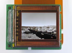
OLED microdisplays improve digital image fusion applications
Grenoble, France--Microdisplay manufacturer MicroOLED demonstrated two prototype 5.4 megapixel, 0.61 inch diagonal organic light-emitting diode (OLED)-based microdisplays in bicolor and tricolor that are designed to improve image resolution and lower the power consumption for night vision and digital image fusion applications in the defense, security, and medical industry.
Digital image fusion—combining video streams from multiple sensors into a single composite image—has important applications in thermal weapon sights, aviator night vision imaging systems and other emerging night sight and situational awareness equipment. Also, surgeons use image fusion systems to integrate and analyze preoperative images to plan and perform brain, spinal, and other complex surgeries. MicroOLED conserves energy in digital image fusion systems by merging the video input signals from multiple sensors directly in the microdisplay rather than the processor.
MicroOLED's bicolor OLED microdisplays can merge a 4.0M pixel image from a night vision sensor with a 1.3M pixel image from a thermal sensor, and its 0.61-inch diagonal is directly compatible with existing systems. The tricolor version enables MicroOLED to merge up to three high resolution images or two images and a graphical overlay, with the following resolutions: a 2.6M pixel B&W image with a 1.3M pixel red image and a 1.3M pixel cyan image. Since the subpixels in the quad-pixel architecture are square, the same shape as pixels used in night vision and thermal sensors, each subpixel can be used as a full pixel. This is unlike the stripe pixel architecture where one needs to use the full color triplet for each pixel.
"MicroOLED's bi- and tricolor OLED microdisplays broaden the performance attributes of our monochrome 5.4M pitch 0.61-inch diagonal microdisplay with a sub-pixel pitch of 4.7 microns by 4.7 microns operating at 0.2W, that we announced earlier this year. This megapixel pitch monochrome microdisplay was well received by professional camera and night vision system makers worldwide, so we are optimistic about the bicolor and tricolor 5.4M dot versions," said Eric Marcellin-Dibon, CEO of MicroOLED."In addition, with our quad pixel architecture, we have increasing flexibility to create new color filter arrangements. These will enable MicroOLED to develop new displays, which will further open up opportunities in the defense and medical markets."
Both optical and digital image fusion systems exist on the market. The strength of optical image fusion is that it can combine images originating from tube intensifiers with a high resolution (up to 2000 pixels) and thermal sensors (up to 1280x1024 pixels) with a fraction of energy, but at the expense of producing a lower quality composite image.
The strength of digital image fusion is that it can record, compress and transmit data, as well as improve the quality of the composite image by adjusting visual parameters. However, it draws more heavily on energy. Current models have a limited image resolution of approximately 1000 lines maximum. For existing models to process images at a higher resolution would require not only increasing the power consumption, but possibly enlarging the display, as well as other system optics, which run counter to the military market trend in Swap (Size, Weight and Power) reductions.
SOURCE: MicroOLED; www.microoled.net/news/news-from-microoled

Gail Overton | Senior Editor (2004-2020)
Gail has more than 30 years of engineering, marketing, product management, and editorial experience in the photonics and optical communications industry. Before joining the staff at Laser Focus World in 2004, she held many product management and product marketing roles in the fiber-optics industry, most notably at Hughes (El Segundo, CA), GTE Labs (Waltham, MA), Corning (Corning, NY), Photon Kinetics (Beaverton, OR), and Newport Corporation (Irvine, CA). During her marketing career, Gail published articles in WDM Solutions and Sensors magazine and traveled internationally to conduct product and sales training. Gail received her BS degree in physics, with an emphasis in optics, from San Diego State University in San Diego, CA in May 1986.
