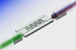
First silicon single-photon source developed by NIST and partners
Gaithersburg, MD--Researchers from the National Institute of Standards and Technology (NIST), the University of California, San Diego (UCSD); and the Politecnico di Milano (Milan, Italy), have demonstrated the first heralded single-photon source made from silicon. NIST says the source complements two other recently developed silicon-based technologies—interferometers for manipulating the entanglement of photons and single photon detectors—needed to build a quantum optical circuit or a secure quantum communication system.
According to NIST scientist Kartik Srinivasan, the new 0.5 mm x 0.05 mm-sized heralded photon generator meshes with existing technology in three important ways: it operates at room temperature; it produces photons compatible with existing telecommunications systems (wavelengths of about 1550 nm); and it is built from silicon using standard, scalable fabrication techniques.
A "heralded" photon is one of a pair whose existence is announced by the detection of its partner—the "herald" photon. To get heralded single photons, the group built upon a technique previously demonstrated in silicon called photon pair generation, wherein a laser pumps photons into a material whose properties cause two incoming pump photons to spontaneously generate a new pair of frequency-shifted photons. However, while these new photons emerge at precisely the same time, it is impossible to know when that will occur. "Detecting one of these photons, therefore, lets us know to look for its partner," says Srinivasan. "While there are a number of applications for photon pairs, heralded pairs will sometimes be needed, for example, to trigger the storage of information in future quantum-based computer memories."
According to Srinivasan, the group's silicon-based device efficiently produced pairs of single photons, and their experiment clearly demonstrated they could herald the presence of one photon by the detection of the other.
While the new device is a step forward, it is not yet practical, according to co-author professor Shayan Mookherjea at UC San Diego, because a single source is not bright enough and a number of other required functions need to be integrated onto the chip. However, putting multiple sources along with their complementary components onto a single chip—something made possible by using silicon-based technology—could supply the performance needed for practical applications. The work was among the three finalists and received an honorable mention in the Maiman Student Paper Competition.
SOURCE: NIST; http://www.nist.gov/public_affairs/tech-beat/tb20120627.cfm#herald

Gail Overton | Senior Editor (2004-2020)
Gail has more than 30 years of engineering, marketing, product management, and editorial experience in the photonics and optical communications industry. Before joining the staff at Laser Focus World in 2004, she held many product management and product marketing roles in the fiber-optics industry, most notably at Hughes (El Segundo, CA), GTE Labs (Waltham, MA), Corning (Corning, NY), Photon Kinetics (Beaverton, OR), and Newport Corporation (Irvine, CA). During her marketing career, Gail published articles in WDM Solutions and Sensors magazine and traveled internationally to conduct product and sales training. Gail received her BS degree in physics, with an emphasis in optics, from San Diego State University in San Diego, CA in May 1986.
