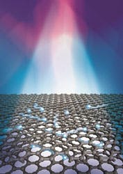
Graphene bolometer from UMD could beat existing IR photodetector technologies
College Park, MD--Unlike semiconductor-based photodetectors, researchers at the Center for Nanophysics and Advanced Materials of the University of Maryland have developed a new type of hot electron bolometer--a sensitive detector of infrared (IR) light--based on bilayer graphene that can be used in a huge range of applications. This bolometer is expected to be sensitive to a very broad range of light energies spanning terahertz frequencies (submillimeter waves) through IR to visible light.
Sensitive detectors of submillimeter waves are being sought for new observatories that will determine the redshifts and masses of very distant young galaxies and enable studies of dark energy and the development of structure in the universe. The graphene bolometer findings are published in the June 3 issue of Nature Nanotechnology.
Photon detectors based on semiconductors absorb photons of light having energies greater than the bandgap energy, a property that forms the basis of devices such as photovoltaic cells. Graphene, however, has a bandgap of exactly zero energy and can absorb photons of any energy, making it an attractive material for absorbing very low energy photons (terahertz and infrared) that pass through most semiconductors. Graphene has another attractive property as a photon absorber: the electrons which absorb the energy are able to retain it efficiently, rather than losing energy to vibrations of the atoms of the material. This same property also leads to extremely low electrical resistance in graphene.
University of Maryland researchers exploited these two properties to devise the hot electron bolometer. It works by measuring the change in the resistance that results from the heating of the electrons as they absorb light.
Normally, graphene's resistance is almost independent of temperature, unsuitable for a bolometer. But when bilayer graphene is exposed to an electric field, it has a small bandgap, large enough that its resistance becomes strongly temperature dependent, but small enough to maintain its ability to absorb low-energy IR photons. By exploiting this method, the bilayer graphene hot electron bolometer operates at a temperature of 5 Kelvin with comparable sensitivity to existing bolometers operating at similar temperatures, but more than a thousand times faster. They extrapolated the performance of the graphene bolometer to lower temperature and found that it may beat all existing technologies.
Some challenges remain. The bilayer graphene bolometer has a higher electrical resistance than similar devices using other materials which may make it difficult to use at high frequencies. Additionally, bilayer graphene absorbs only a few percent of incident light. But the Maryland researchers are working on ways to get around these difficulties with new device designs, and are confident that a graphene has a bright future as a photodetector material.
SOURCE: University of Maryland; www.newsdesk.umd.edu/mail/mail_form.cfm?ArticleID=2706

Gail Overton | Senior Editor (2004-2020)
Gail has more than 30 years of engineering, marketing, product management, and editorial experience in the photonics and optical communications industry. Before joining the staff at Laser Focus World in 2004, she held many product management and product marketing roles in the fiber-optics industry, most notably at Hughes (El Segundo, CA), GTE Labs (Waltham, MA), Corning (Corning, NY), Photon Kinetics (Beaverton, OR), and Newport Corporation (Irvine, CA). During her marketing career, Gail published articles in WDM Solutions and Sensors magazine and traveled internationally to conduct product and sales training. Gail received her BS degree in physics, with an emphasis in optics, from San Diego State University in San Diego, CA in May 1986.
