Integrated-optics foundry service OpSIS conducts first multiuser run
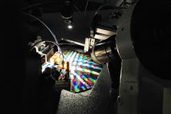
Newark, DE--The Optoelectronic Systems Integration in Silicon (OpSIS) foundry, founded at the University of Delaware (UD), conducted its first multiuser run earlier this month (Oct. 2012), creating 200-mm-diameter silicon wafers embedded with more than thirty unique photonics devices per die; this master design was replicated 30 or more times across the wafer, producing in excess of 1000 photonics devices on each silicon substrate.
The devices include couplers, modulators, waveguides, and other photonic components that route, control, and manipulate light. Using “shuttle runs,” OpSIS can significantly reduce costs of building new silicon photonics devices, bringing prototyping capability for leading-edge photonics within reach of startups and academic research groups.
The OpSIS foundry was established by UD professor Michael Hochberg, who is also known as a founder of the silicon-photonics company Luxtera (Carlsbad, CA).
At UD, Hochberg’s research team is conducting quality-control testing on the multiuser run to ensure that the optical circuits embedded in the silicon wafers perform as expected. Test structures built into the chips are used to isolate any nonperforming devices to determine if fabrication errors exist and to resolve problems for future production runs.
“We are building the next wave in photonic circuits,” says Hochberg. "Using a foundry service to aggregate different requests from smaller organizations, we are making it accessible to researchers, who previously wouldn’t have access, to test new ideas and devices—work that may lead to future advances in photonics."
“The semiconductor industry has used the fabless manufacturing model, with specialized dedicated foundries performing the actual fabrication, for close to 50 years,” says John Wright, a researcher involved in the project. “We’re taking a well-established concept and tool set and applying it to photonics.”
Source: http://www.udel.edu/udaily/2013/oct/hochberg-photonics-101712.html

John Wallace | Senior Technical Editor (1998-2022)
John Wallace was with Laser Focus World for nearly 25 years, retiring in late June 2022. He obtained a bachelor's degree in mechanical engineering and physics at Rutgers University and a master's in optical engineering at the University of Rochester. Before becoming an editor, John worked as an engineer at RCA, Exxon, Eastman Kodak, and GCA Corporation.
