Prototype thin-film IR-emitting chip sets efficiency record for Osram
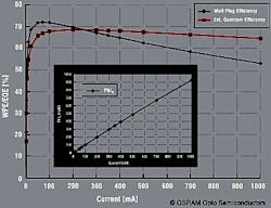
Regensberg, Germany--A 1 mm2 infrared (IR)-emitting prototype chip from Osram Opto Semiconductors has reached an efficiency of up to 72% at a 100 mA current at room temperature using thin-film technology. At 930 mW from a DC operating current of 1 A, its light output under laboratory conditions is 25% higher than that of the chips currently available on the market, says Osram.
The efficiency is true wall-plug efficiency, or the ratio of the radiated power to the electrical input power. The prototype has a quantum efficiency that remains around 65% up to 1 A. The 850 nm emission is useful particularly for surveillance tasks and use with CCTV cameras. There are also potential safety applications in the automotive sector, such as precrash sensors and illumination sources for night-vision systems.
“The way in which the efficiency and brightness have been increased can be transferred from 850 nm to other wavelengths,” says Markus Bröll, project manager for the development of IRED chips at Osram Opto Semiconductors in Regensburg. “This means that it will be possible to create highly energy-efficient solutions for infrared lighting in the future." Fewer components will be needed in multi-chip applications, he notes, saving both money and energy.
The new chip is expected to go into series production by the middle of 2013.

John Wallace | Senior Technical Editor (1998-2022)
John Wallace was with Laser Focus World for nearly 25 years, retiring in late June 2022. He obtained a bachelor's degree in mechanical engineering and physics at Rutgers University and a master's in optical engineering at the University of Rochester. Before becoming an editor, John worked as an engineer at RCA, Exxon, Eastman Kodak, and GCA Corporation.
