Bodkin lands Air Force hyperspectral imaging contract
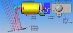
Newton, MA--The US Air Force Research Lab (ARL) has awarded Bodkin Design & Engineering a $150,000 contract to develop a high-spatial-resolution hyperspectral sensor operating in the longwave-infrared (LWIR) spectral band. A prototype of the imaging spectroscopy system will be demonstrated as part of ARL’s efforts to improve target acquisition and threat assessment to protect civilian and military assets.
Hyperspectral imaging combines the spatial image with spectral analysis to build up a three-dimensional data-cube (two dimensions of the data-cube are spatial and the third dimension is wavelength). There are several methods currently available for acquiring hyperspectral images, but they are limited in their ability to satisfy the military’s need for speed, accuracy, and data rate.
Bodkin says the hyperspectral imaging device will capture spectral and spatial information with unprecedented data-cube size and speed, which will improve standoff target detection, materials identification, and the quantification of atmospheric constituents and effluents. Key applications include missile defense, chemical defense, autonomous material identification, and homeland security.
The 9-month-long project is funded under the Small Business Innovation Research (SBIR) program. Bodkin Design & Engineering provides concept development, and design and build services to the OEM, commercial, military, and research communities.

Conard Holton
Conard Holton has 25 years of science and technology editing and writing experience. He was formerly a staff member and consultant for government agencies such as the New York State Energy Research and Development Authority and the International Atomic Energy Agency, and engineering companies such as Bechtel. He joined Laser Focus World in 1997 as senior editor, becoming editor in chief of WDM Solutions, which he founded in 1999. In 2003 he joined Vision Systems Design as editor in chief, while continuing as contributing editor at Laser Focus World. Conard became editor in chief of Laser Focus World in August 2011, a role in which he served through August 2018. He then served as Editor at Large for Laser Focus World and Co-Chair of the Lasers & Photonics Marketplace Seminar from August 2018 through January 2022. He received his B.A. from the University of Pennsylvania, with additional studies at the Colorado School of Mines and Medill School of Journalism at Northwestern University.
