(Image: UPC)
Barcelona, Spain--A group at the Nanoengineering Research Centre (CRNE) and the Department of Electronic Engineering at the Universitat Politècnica de Catalunya (UPC) has found a way to make the manufacture of silicon-based devices such as photovoltaic (PV) solar cells more affordable. The results of their research have recently been published in the online version of Applied Physics Letters.
If ultrathin (on the order of 10 µm) silicon (Si) wafers could be made via some sort of low-cost manufacturing process, money would be saved on the making of solar cells, computer circuits, and other Si-based devices; the reason is that the Si itself is a significant portion of the cost of making such devices, so the thinner that Si can be sliced, the better.
Today's waste, tomorrow's economy
In recent years, techniques have been developed to obtain increasingly thinner crystalline silicon wafers from monocrystalline cylindrical ingots. Layers cut from the ingots using a multithreaded saw impregnated with abrasive material have a minimum thickness of around 150 µm. Obtaining wafers that are any thinner is more complicated, as existing methods only allow such wafers to be obtained one at a time. Furthermore, 50% of the silicon is lost in the process.
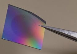
The technology developed by the UPC team enables a large number of crystalline layers, controlled for thickness, to be produced from a single crystalline silicon wafer in a single step. The outcome is a sort of crystalline silicon "millefeuille" (which is a many-layered pastry) produced more efficiently, more rapidly, and more affordably than by existing methods.
The researchers create small pores in Si and apply a high temperature; multiple separate crystalline silicon wafers are obtained by carefully controlling the pore profiles. Precise control over diameter controls both the number of layers and their thickness. The millefeuille silicon layers are then separated by exfoliation (or so-called "peeling"). The resulting number of silicon layers is determined by the thickness of the layers themselves and the initial thickness of the wafer. The researchers have succeeded in creating up to 10 thin wafers 5 to 7 µm thick from a single 300 µm thick wafer.
A note on PV cells: the researchers showed that, despite the lesser thickness, the wafers retain a high capacity to absorb solar energy and convert it into electricity.
