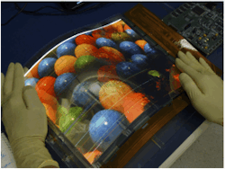
Tempe, AZ--Arizona State University's Flexible Electronics and Display Center (FEDC) has successfully manufactured the world's largest flexible color organic light-emitting display (OLED) prototype using mixed-oxide thin-film transistors (TFTs). Measuring 14.7 diagonal inches (nearly twice as large as the previous record-setting device developed by the FDC), the device was developed at the FEDC in conjunction with Army Research Labs scientists.
"Mixed oxide TFTs offer a highly cost-effective approach for manufacturing displays that deliver high performance, including vibrant colors, high switching speeds for video and reduced power consumption - all features that will be required for the next generation of consumer electronics," said Nick Colaneri, Director of the FEDC. "Furthermore, mixed oxide TFTs can be manufactured on existing amorphous silicon production lines, eliminating the need for specialized equipment and processing, thereby reducing costs compared to competitive approaches."
The new device also meets a critical target set by the U.S. Department of Defense to advance the development of full-color, full-motion video flexible OLED displays (http://www.laserfocusworld.com/articles/print/volume-45/issue-1/features/flexible-displays-metal-foil-backed-oled-displays-will-soon-be-rollable.html) for use in thin, lightweight, bendable and highly rugged devices. This latest version includes advancements in both the OLED materials to enhance performance as well as the encapsulation processes used to protect the display.
SOURCE: The Flexible Electronics and Display Center; http://flexdisplay.asu.edu/

Gail Overton | Senior Editor (2004-2020)
Gail has more than 30 years of engineering, marketing, product management, and editorial experience in the photonics and optical communications industry. Before joining the staff at Laser Focus World in 2004, she held many product management and product marketing roles in the fiber-optics industry, most notably at Hughes (El Segundo, CA), GTE Labs (Waltham, MA), Corning (Corning, NY), Photon Kinetics (Beaverton, OR), and Newport Corporation (Irvine, CA). During her marketing career, Gail published articles in WDM Solutions and Sensors magazine and traveled internationally to conduct product and sales training. Gail received her BS degree in physics, with an emphasis in optics, from San Diego State University in San Diego, CA in May 1986.
