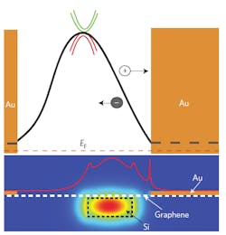
Graphene could bridge a key gap in the development of silicon photonics for the fiber transmission band. Silicon photodetectors are limited to wavelengths shorter than about 1.1 µm, so other materials must be added to reach the longer wavelengths in the fiber band. Now, three independent groups report making photodetectors with high responsivity at wavelengths from 1.3 to 2.75 µm by integrating graphene sheets with silicon waveguides.
Lacking a bandgap, graphene absorbs uniformly across a broad range in the visible and infrared, but getting the the single-atomic-layer sheets to absorb enough light to make useful detectors has been challenging. A key innovation in breaking that barrier is integrating the graphene layer with a silicon waveguide that guides photons along the length of the graphene. The evanescent field from the waveguide excites carriers in the graphene, and the geometry increases the total absorption—and responsivity—without increasing response time or limiting speed.Nature Photonics published all three reports online on September 15, 2013. The overall results are similar in many ways, including their compatibility with CMOS fabrication technology, but their approaches differ in details. Operation of detectors with graphene coating the top and sides of raised silicon waveguides at wavelengths of 1.3 to 1.65 µm and 3 dB bandwidth of 18 GHz was reported by Andreas Pospischil of the Vienna University of Technology (Vienna, Austria) and colleagues. Photodetection by graphene/silicon heterostructure waveguide structures on a direct transition at 1.55 µm and an indirect transition at 2.75 µm was reported by Xiaomu Wang and colleagues of the Chinese University of Hong Kong. (Hong Kong, China) Operation of a metal-doped graphene junction photodetector at speeds exceeding 20 GHz at wavelengths between 1.45 and 1.59 µm, and in a 12 Gbit/s data link, was reported by Xuetao Gan of Columbia University (New York, NY) and colleagues.
As noted in the papers, and in a commentary by Ming Liu and Xiang Zhang of the University of California (Berkeley, CA), plenty of work remains to make a practical technology. A key issue is developing a graphene-deposition technique more amenable to mass production of detectors than the current "exfoliation" approach based on manually peeling layers of graphene. But with multiple approaches already demonstrated, and photoresponsivity reaching 0.13 A/W, integration of graphene with silicon waveguides is looking very promising.

Jeff Hecht | Contributing Editor
Jeff Hecht is a regular contributing editor to Laser Focus World and has been covering the laser industry for 35 years. A prolific book author, Jeff's published works include “Understanding Fiber Optics,” “Understanding Lasers,” “The Laser Guidebook,” and “Beam Weapons: The Next Arms Race.” He also has written books on the histories of lasers and fiber optics, including “City of Light: The Story of Fiber Optics,” and “Beam: The Race to Make the Laser.” Find out more at jeffhecht.com.
