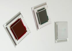
NikkoIA SAS announces several development programs for organic near-infrared imaging
Moirans/Grenoble, France--NikkoIA SAS has received grants through Europe’s FP7 Framework Programme for several collaborative development programs in 2013, totaling about 1.5 million Euros of cumulated subsidies over the next two years.
One project, called “Organic Semiconductors for NIR Optoelectronics," involves the development of new organic materials sensitive in the near-infrared (NIR) spectral region. The objective is to extend NIR-photosensitive organic-semiconductor materials to be used for sensors and photodetectors with tunable sensitivity windows. It includes synthesis, characterization, and application of NIR-absorbing and emitting organic materials.
The other granted programs, which are more product-oriented, are dedicated to the development of organic image sensors based either on amorphous silicon (a-Si) active-matrix thin-film-transistor (TFT) backplanes or silicon CMOS substrates, targeting specific applications such as biometrics, medical, and security of goods and people.
“[This grant] secures our development roadmap for the next two years," says Alain Jutant, president of NikkoIA.

John Wallace | Senior Technical Editor (1998-2022)
John Wallace was with Laser Focus World for nearly 25 years, retiring in late June 2022. He obtained a bachelor's degree in mechanical engineering and physics at Rutgers University and a master's in optical engineering at the University of Rochester. Before becoming an editor, John worked as an engineer at RCA, Exxon, Eastman Kodak, and GCA Corporation.
