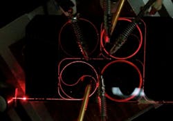
50 m of ultra-low-loss optical delay placed on a single microchip
Santa Barbara and Pasadena, CA--For adding a true time delay to a photonic circuit, nothing is better than an actual length of optical fiber or other optical waveguide (as opposed to "slow-light" techniques, which are less robust, can have narrow functional bands, and can be quite complex). Conventionally, coiled optical fiber is used; a 50 m length of coiled optical fiber takes a space about as large as a juice glass. Now, scientists funded by the U.S. Defense Advanced Research Projects Agency (DARPA) integrated Photonic Delay (iPhoD) program have created chip-based photonic waveguides with ultralow losses, managing to pack up to 50 m of optical delay onto a single microchip.
0.05 dB/m loss
One of the big breakthroughs is actually the low optical loss of these new chip-based waveguides. “Prior to the start of iPhoD, the best integrated waveguides had a signal loss of about 1 decibel per meter with total lengths of only a few meters,” says Josh Conway, DARPA program manager. “Under iPhoD, two research teams created chips with loss around 0.05 decibels per meter. The submillimeter bend diameter, which describes how tightly the waveguide can coil without significant signal loss, allowed the demonstration of a 50-meter optical delay on a single microchip.”
The ability to use on-chip waveguides rather than off-chip optical fiber for delays has another great advantage: the elimination of bulky, sensitive, labor-intensive waveguide-to-fiber couplers.
Two material-systems approaches
iPhoD concluded recently with successful demonstrations by research teams led by the University of California, Santa Barbara (UCSB) and the California Institute of Technology (CalTech).
The ultra-low-loss, true-time delay chip developed at UCSB is composed of silicon nitride. Selecting this material may allow for integration with a variety of devices and materials, reducing size, weight, and power requirements of an overall system. UCSB researchers also demonstrated 3D waveguide stacking, enabling more waveguide length and thus longer photonic delays.
Researchers at CalTech had a different approach for a chip-scale waveguide, as reported in a Nature Communications paper, “Ultra-low-loss optical delay line on a silicon chip.” The CalTech waveguide was constructed from silicon oxide, commonly known as glass, and demonstrated low loss over 27 m.
“Chip-scale waveguides, with smaller sizes and new integration possibilities promise advanced, compact military systems such as tactical gyroscopes that significantly outperform state-of-the-art MEMS devices with the same footprint," notes Conway.
Source: http://www.darpa.mil/NewsEvents/Releases/2013/11/26.aspx

John Wallace | Senior Technical Editor (1998-2022)
John Wallace was with Laser Focus World for nearly 25 years, retiring in late June 2022. He obtained a bachelor's degree in mechanical engineering and physics at Rutgers University and a master's in optical engineering at the University of Rochester. Before becoming an editor, John worked as an engineer at RCA, Exxon, Eastman Kodak, and GCA Corporation.
