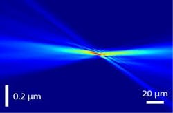
Lens developed for hard x-ray nanoprobe beamline achieves 11 nm focal spot
Upton, NY--At the National Synchrotron Light Source II (NSLS-II) now under construction at Brookhaven National Laboratory (BNL), 12 keV x-rays produced by the Hard X-ray Nanoprobe beamline (HXN) have now been focused down to an 11 nm spot size.1 The BNL researchers used a novel x-ray optic called a multilayer Laue lens (MLL), which consists of nested approximately cylindrical layers that focus hard x-rays via grazing incidence.
The researchers analyzed their MLL's focusing performance using a technique known as ptychography. "With ptychography, we can visualize how the x-rays are traveling from the lens to the focus and to an arbitrary point in the optical path. Therefore, we do not have to use conventional knife-edge scans to quantify lens aberrations," says Xiaojing Huang, one of the researchers. The ptychography analysis quantified the lens aberrations at a 0.3 wave period, very close to a quarter wave period. This represents a rigorous threshold value for "diffraction-limited" focusing.
The NSLS-II will enable scientists to image structures at ever-smaller spatial scales. HXN's long-range goal is to achieve a resolution of 1 nm. Hard x-rays exhibit excellent structural, elemental and chemical sensitivity and are particularly suited for in-situ studies that are challenging for electrons.
The Brookhaven-fabricated MLL has a 43-micron aperture (the largest yet reported MLL size). It accepts substantially more x-rays than earlier MLLs and offers a significantly larger working distance, needed for in-situ experiments. It also contains a total of 6,510 layers, with thicknesses ranging from 4 to 21 nm.
Source: http://www.bnl.gov/newsroom/news.php?a=24676
REFERENCE:
1. Xiaojing Huang et al., Scientific Reports 3, Article number: 3562. DOI: 10.1038/srep03562

John Wallace | Senior Technical Editor (1998-2022)
John Wallace was with Laser Focus World for nearly 25 years, retiring in late June 2022. He obtained a bachelor's degree in mechanical engineering and physics at Rutgers University and a master's in optical engineering at the University of Rochester. Before becoming an editor, John worked as an engineer at RCA, Exxon, Eastman Kodak, and GCA Corporation.
