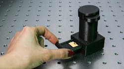
LED-based lab-on-a-chip device screens for 170,000 molecules in blood
Ecole polytechnique fédérale de Lausanne (EPFL; Lausanne, Switzerland) researchers have developed a new light-emitting diode (LED)-based handheld device that is able to test a large number of proteins in our body all at once. Professor Hatice Altug and postoctoral fellow Arif Cetin from EPFL in collaboration with professor Aydogan Ozcan from UCLA (Los Angeles, CA) developed the compact and inexpensive "optical lab on a chip" to quickly analyze up to 170,000 different molecules in a blood sample—simultaneously identifying insulin levels, cancer and Alzheimer markers, or even certain viruses.
Instead of analyzing the biosample by looking at the spectral properties of the sensing platforms as has traditionally been the case, this new technique uses changes in the intensity of the light to do on-chip imaging, eliminating sometimes clunky spectrometers in the process.
RELATED ARTICLE: Lensless optical microscope on a chip uses tomography to produce high-resolution 3-D images
Only 7.5 cm high and weighing 60 g, the device is able to detect viruses and single-layer proteins down to 3 nanometers thick. Detailed in a publication in Nature Light: Science & Application, the recipe is simple and contains few ingredients: an off-the-shelf CMOS chip, an LED, and a 10 square millimeter gold plate pierced with arrays of extremely small holes less than 200 nm wide.
Nanoholes on the gold substrates are compartmented into arrays of different sections, where each section functions as an independent sensor. Sensors are coated with special biofilms that are specifically attracting targeted proteins. Consequently, multiple different proteins in the biosamples could be captured at different places on the platform and monitored simultaneously. The LED light shines on the platform, passes through the nanoscale openings and its properties are recorded onto the CMOS chip. Since light going through the nanoscale holes changes its properties depending on the presence of biomolecules, it is possible to easily deduce the number of particles trapped on the sensors.
Laboratories normally observe the difference between the original wavelength and the resulting one, but this requires using sometimes bulky spectrometers. Hatice Altug's ingenuity consists in choosing to ignore the light's wavelength, or spectrum, and focus on changes in the light intensity instead. This method is possible by tuning into the "surface plasmonic resonance"—the collective oscillation of electrons when in contact with light. And this oscillation is very different depending on the presence or absence of a particular protein. Then, the CMOS chip only needs to record the intensity of the oscillation.
The size, price, and efficiency of this new multi-analyze device make it a highly promising invention for a multiplicity of uses. "Recent studies have shown that certain illness like cancer or Alzheimer's are better diagnosed and false positive results avoided when several parameters can be analyzed at once," says Hatice Altug. The research team foresees collaborating with local hospitals in the near future to find the best way to use this new technology.
SOURCE: EPFL; http://actu.epfl.ch/news/a-complete-medical-check-up-on-a-chip/

Gail Overton | Senior Editor (2004-2020)
Gail has more than 30 years of engineering, marketing, product management, and editorial experience in the photonics and optical communications industry. Before joining the staff at Laser Focus World in 2004, she held many product management and product marketing roles in the fiber-optics industry, most notably at Hughes (El Segundo, CA), GTE Labs (Waltham, MA), Corning (Corning, NY), Photon Kinetics (Beaverton, OR), and Newport Corporation (Irvine, CA). During her marketing career, Gail published articles in WDM Solutions and Sensors magazine and traveled internationally to conduct product and sales training. Gail received her BS degree in physics, with an emphasis in optics, from San Diego State University in San Diego, CA in May 1986.
