Quantum-cascade structure and metamaterial combine to make sensitive mid-IR and terahertz detector
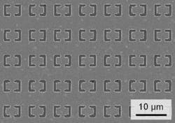
Scientists at Technische Universität Wien (TUW) have discovered that a semiconductor structure identical to that of a conventional terahertz-emitting quantum-cascade laser (QCL) can, with the addition of a 2D metamaterial pattern pressed into its top-layer metal contact, be used as a sensitive mid-IR and terahertz photodetector.1 When used to detect terahertz radiation, the as-fabricated device is more than a thousand times thinner than the wavelength of the light being detected.
Efficient coupling
The metamaterial allows the terahertz or mid-IR radiation to be efficiently coupled to the gallium arsenide (GaAs)-based QCL structure; wavelengths both below and above the reststrahlen band of GaAs can be coupled. (The reststrahlen band is a narrow reflective band with a wavelength tied to the semiconductor properties; for GaAs it is on the order of 37 µm.)
"Ultrathin layered semiconductor systems have the great advantage that their electronic properties can be very precisely tuned," says Karl Unterrainer, one of the TUW researchers. One problem, however, is that quantum physics prohibits photons with a certain polarization from interacting with the electrons of the semiconductor system. Light that hits the layered surface head-on cannot influence the electrons in the semiconductor. Therefore a method is required to rotate the polarization of the incident light so that it can be detected in the semiconductor layers; in the TUW device, this is done with the 2D metamaterial.
The discovery opens up the possibility of integrating a light detector for terahertz radiation into a chip. "With conventional fabrication methods, large arrays of such detectors can be built," says Unterrainer.
Source: https://www.tuwien.ac.at/en/news/news_detail/article/8708/
REFERENCE:
A. Benz et al., Nature Scientific Reports (2014); doi: 10.1038/srep04269

John Wallace | Senior Technical Editor (1998-2022)
John Wallace was with Laser Focus World for nearly 25 years, retiring in late June 2022. He obtained a bachelor's degree in mechanical engineering and physics at Rutgers University and a master's in optical engineering at the University of Rochester. Before becoming an editor, John worked as an engineer at RCA, Exxon, Eastman Kodak, and GCA Corporation.
