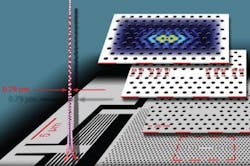
Physicists at the University of Rochester (Rochester, NY), Ecole Polytechnique Federale de Lausanne (Lausanne, Switzerland), and the Universita di Pavia (Pavia, Italy) have created a silicon nanocavity that allows light to be trapped ten times longer than in other similarly-sized optical cavities.1 The cavity had a quality factor Q of 2 × 10⁶.
The nanocavity—a nanostructured region of a silicon wafer—holds light for a period of nanoseconds. Typically light would travel several meters in that time, but instead the nanostructure confined light in a micrometer-sized region. Such nanostructures can be important components in nanophotonics circuits.
Until now, researchers have been using educated-guess procedures to design light-trapping nanostructures. However, in this case, the researchers used a numerical technique that lead to the design improvement. Their computational approach allowed them to search for the optimal combination of parameters among thousands of realizations using a genetic algorithm.
The principle behind the genetic approach is to regard each new nanocavity as an individual in a population. The individuals mutate and "breed," meaning that two single structures combine to create a new one that is a cross between the two "parents." As new generations succeeded one another, the algorithm selected the fittest ones in each generation, in this case, the ones that exhibited the longest trapping time (the highest quality factor).
The results shown by Antonio Badolato, professor of physics at the University of Rochester, and his colleagues demonstrate one of the highest quality factors ever measured in nanocavities while maintaining a very small footprint.
Biosensing uses
The extreme sensitivity of these nanocavities to tiny changes in the environment—for example, a virus attaching near the area where light is trapped—makes these devices particularly appealing for biosensing. Badolato's group is now starting a collaboration with researchers at the University of Rochester's Medical Center to exploit this interesting property with the new nanocavities.
REFERENCE:
1. Y. Lai et al., Applied Physics Letters (2014); doi: 10.1063/1.4882860

John Wallace | Senior Technical Editor (1998-2022)
John Wallace was with Laser Focus World for nearly 25 years, retiring in late June 2022. He obtained a bachelor's degree in mechanical engineering and physics at Rutgers University and a master's in optical engineering at the University of Rochester. Before becoming an editor, John worked as an engineer at RCA, Exxon, Eastman Kodak, and GCA Corporation.
