Horiba Scientific to display back-illuminated, deep-cooled CCD camera at SPIE Optics + Photonics 2014

Aug. 5, 2014
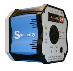
The Syncerity back-illuminated, deep-cooled CCD camera with a near-infrared (NIR)-enhanced, 2048 × 70 sensor offers high-resolution, 14 µm pixel size, ultralow etaloning, and more than 40% quantum efficiency at 1000 nm.

The Syncerity back-illuminated, deep-cooled CCD camera with a near-infrared (NIR)-enhanced, 2048 × 70 sensor offers high-resolution, 14 µm pixel size, ultralow etaloning, and more than 40% quantum efficiency at 1000 nm. Lifetime vacuum warranty and compact size make it ideal for OEM integration, particularly in Raman microscopes, and its flexible design allows the company's OEM-dedicated team to quickly adapt the camera for industrial applications.

SPIE Optics + Photonics booth number: 328

To Learn More:

Contact:Horiba Scientific
Headquarters: Edison, NJ
Product: Syncerity back-illuminated, deep-cooled CCD camera
Key Features: 14 µm pixel size and ultralow etaloning

What Horiba Scientific says:
View more information on the Syncerity back-illuminated, deep-cooled CCD camera.

View More Products
Locate a vendor or system integrator in our Buyer's Guide.

Share new products that you think are particularly interesting or helpful by contacting Lee Dubay, Associate Editor, Laser Focus World.
Sponsored Recommendations

Brain Computer Interface (BCI) electrode manufacturing

Jan. 31, 2025
Learn how an industry-leading Brain Computer Interface Electrode (BCI) manufacturer used precision laser micromachining to produce high-density neural microelectrode arrays.

Electro-Optic Sensor and System Performance Verification with Motion Systems

Jan. 31, 2025
To learn how to use motion control equipment for electro-optic sensor testing, click here to read our whitepaper!

How nanopositioning helped achieve fusion ignition

Jan. 31, 2025
In December 2022, the Lawrence Livermore National Laboratory's National Ignition Facility (NIF) achieved fusion ignition. Learn how Aerotech nanopositioning contributed to this...

Nanometer Scale Industrial Automation for Optical Device Manufacturing

Jan. 31, 2025
In optical device manufacturing, choosing automation technologies at the R&D level that are also suitable for production environments is critical to bringing new devices to market...

Voice your opinion!

To join the conversation, and become an exclusive member of Laser Focus World, create an account today!