Thinnest-possible heterostructures created for next generation of LEDs, laser diodes
Scientists from the University of Washington (UW; Seattle, WA), the University of Warwick (Coventry, England), and the University of Hong Kong have created what they say is the thinnest-possible semiconductor heterostructure, a new class of nanoscale materials made in sheets only three atoms thick.1
The researchers have demonstrated that two single-layer semiconductor materials can be connected in an atomically seamless fashion to produce a heterojunction. This result, which allows band engineering within the 2D plane, could be the basis for next-generation flexible and transparent computing, better LEDs and laser diodes, and new solar technologies.
Two flat semiconductor materials were connected edge-to-edge in an undistorted honeycomb lattice (in other words, perfect crystalline alignment). The researchers worked with two monolayer materials—molybdenum diselenide (MoSe2) and tungsten diselenide WSe2)—that have very similar structures, which was key to creating the composite 2D semiconductor. The structures were grown by lateral heteroepitaxy via physical vapor transport.
Active photojunction
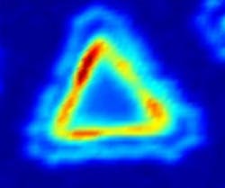
The researchers have already demonstrated that the junction interacts with light much more strongly than the rest of the monolayer, which is encouraging for optoelectric and photonic applications like solar cells.
With a larger furnace, it would be possible to mass-produce sheets of these semiconductor heterostructures, the researchers say. On a small scale, it takes about five minutes to grow the crystals, with up to two hours of heating and cooling time.
"This is a scalable technique," says Sanfeng Wu, a UW doctoral student in physics and one of the lead authors. "Because the materials have different properties, they evaporate and separate at different times automatically. The second material forms around the first triangle that just previously formed. That's why these lattices are so beautifully connected."
REFERENCE:
1. Chunming Huang et al., Nature Materials (2014); doi: 10.1038/nmat4064

John Wallace | Senior Technical Editor (1998-2022)
John Wallace was with Laser Focus World for nearly 25 years, retiring in late June 2022. He obtained a bachelor's degree in mechanical engineering and physics at Rutgers University and a master's in optical engineering at the University of Rochester. Before becoming an editor, John worked as an engineer at RCA, Exxon, Eastman Kodak, and GCA Corporation.
