AMO GmbH demos ultrafast graphene-based photodetectors with data rates up to 50 Gbit/s
In cooperation with Alcatel Lucent Bell Labs (Boulogne-Billancourt, France), researchers from AMO GmbH (Aachen, Germany) have created what they say is the world's fastest graphene-based photodetector, operating at a maximum data rate of 50 Gbit/s.1
Graphene, a two-dimensional layer of carbon atoms, is a promising material for future ultrafast and compact telecommunication systems -- not least because it can be integrated into large-scale silicon based systems that combine optics and electronics. Graphene also has a very high charge-carrier mobility and a broadband electro-optical response.
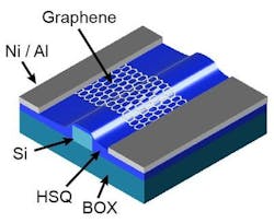
In the AMO/Alcatel work, graphene-based photodetectors were integrated in a conventional silicon-photonic platform designed for future on-chip applications for ultrafast data communications. The platform took advantage of graphene's characteristics such as dark-current-free, high speed operation and potential CMOS-compatible large-scale integration.
-3 dB bandwidth of 41 GHz
The graphene was grown on silicon photonic waveguides using chemical vapor deposition (CVD); the resulting device operates with no bias at 1550 nm with an extrinsic -3 dB bandwidth of 41 GHz and operability up to 50 GHz with excellent signal integrity, according to the researchers.
The work was supported by the European Commission through the Flagship project "Graphene" and the integrated project "Grafol," as well as the DPG supported project "GraTiS."
Source: http://www.amo.de/21.0.html?&L=1&tx_ttnews[tt_news]=297&tx_ttnews[backPid]=8&cHash=475793e5f9&L=2
REFERENCE:
1. Daniel Schall et al., ACS Photonics, Article ASAP (2014); doi: 10.1021/ph5001605

John Wallace | Senior Technical Editor (1998-2022)
John Wallace was with Laser Focus World for nearly 25 years, retiring in late June 2022. He obtained a bachelor's degree in mechanical engineering and physics at Rutgers University and a master's in optical engineering at the University of Rochester. Before becoming an editor, John worked as an engineer at RCA, Exxon, Eastman Kodak, and GCA Corporation.
