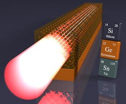
Group IV germanium-tin laser compatible with silicon chips
Forschungszentrum Jülich (Jülich, Germany) and Paul Scherrer Institute (PSI; Villigen PSI, Switzerland) scientists in cooperation with international partners have presented the first semiconductor consisting solely of group IV elements (see Nature Photonics, DOI: 10.1038/NPHOTON.2014.321). As a consequence, the germanium-tin (GeSn) laser can be applied directly onto a silicon chip, creating a new basis for transmitting data on computer chips via light.
RELATED ARTICLE: Can germanium replace silicon in mid-infrared group IV photonics?
The basis of chip manufacturing is silicon, an element of the main group IV section of the periodic table. Typical semiconductor lasers for telecommunication systems, made of gallium arsenide for example, are costly and consist of elements from the main groups III or V. This has profound consequences on the crystal properties. Such laser components cannot therefore be applied directly onto silicon. They have to be produced externally at great effort and subsequently glued to the silicon wafer. However, the lifetime of this kind of component is greatly reduced due to the fact that the thermal expansion coefficients of these elements are significantly different from that of silicon.
In contrast, group IV semiconductors—to which both silicon and germanium belong—can be integrated into the manufacturing process without any major difficulties. Neither element is very efficient as a light source, however. They are classed among the indirect semiconductors. In contrast to direct semiconductors, they emit mostly heat and only a little light when excited. That is why research groups all over the globe are intensively pursuing the objective of manipulating the material properties of germanium so that it would be able to amplify optical signals and thus make it a usable laser source.
The scientists at Jülich's Peter Grünberg Institute have now for the first time succeeded in creating a "real" direct main group IV semiconductor laser by combining germanium and tin, which is also classed in main group IV. "The high tin content is decisive for the optical properties. For the first time, we were able to introduce more than 10% tin into the crystal lattice without it losing its optical quality," reports PhD student Stephan Wirths. "The functioning of the laser is so far limited to low temperatures of up to minus 183 degrees Celsius, however. This is mainly due to the fact that we worked with a test system that was not further optimized," adds Buca.
The laser was excited optically for the demonstration. Currently, the scientists in Dan Buca's group at Jülich are working on linking optics and electronics even more closely. The next big step forward will be generating laser light with electricity instead, and without the need for cooling if possible. The aim is to create an electrically pumped laser that functions at room temperature.
The laser beam is not visible to the naked eye. GeSn absorbs and emits light in a wavelength range of about 3 microns. Along with computer chips, completely new applications that have not been pursued so far for financial reasons may thus benefit from the new laser material. Gas sensors or implantable chips for medical applications which can gather information about blood sugar levels or other parameters via spectroscopic analysis are examples. In the future, cost-effective, portable sensor technology—which may be integrated into a smart phone—could supply real-time data on the distribution of substances in the air or the ground and thus contribute to a better understanding of weather and climate development.
SOURCE: Forschungszentrum Jülich; http://www.fz-juelich.de/SharedDocs/Pressemitteilungen/UK/EN/2015/15-01-19gesn-laser.html;jsessionid=2BA38FB5C6DB2797FB23167966BC0502
About the Author

Gail Overton
Senior Editor (2004-2020)
Gail has more than 30 years of engineering, marketing, product management, and editorial experience in the photonics and optical communications industry. Before joining the staff at Laser Focus World in 2004, she held many product management and product marketing roles in the fiber-optics industry, most notably at Hughes (El Segundo, CA), GTE Labs (Waltham, MA), Corning (Corning, NY), Photon Kinetics (Beaverton, OR), and Newport Corporation (Irvine, CA). During her marketing career, Gail published articles in WDM Solutions and Sensors magazine and traveled internationally to conduct product and sales training. Gail received her BS degree in physics, with an emphasis in optics, from San Diego State University in San Diego, CA in May 1986.
