Quantum computing gets boost from MIT on-chip single-photon detector arrays
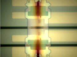
A team of researchers has built an on-chip array of light detectors sensitive enough to register the arrival of individual photons. Such arrays are crucial components of devices that use photons to perform quantum computations; however, single-photon detectors are notoriously temperamental: Of 100 deposited on a chip using standard manufacturing techniques, only a handful will generally work. In a paper in Nature Communications, the researchers at MIT and elsewhere describe a procedure for fabricating and testing the detectors separately and then transferring those that work to an optical chip built using standard manufacturing processes.
RELATED ARTICLE: Quantum computing poses challenges
In addition to yielding much denser and larger arrays, the approach also increases the detectors' sensitivity. In experiments, the researchers found that their detectors were up to 100 times more likely to accurately register the arrival of a single photon than those found in earlier arrays.
With most particles, entanglement is difficult to maintain, but it’s relatively easy with photons. For that reason, optical systems are a promising approach to quantum computation. But any quantum computer--say, one whose qubits are laser-trapped ions or nitrogen atoms embedded in diamond--would still benefit from using entangled photons to move quantum information around.
"Because ultimately one will want to make such optical processors with maybe tens or hundreds of photonic qubits, it becomes unwieldy to do this using traditional optical components," says Dirk Englund, the Jamieson Career Development Assistant Professor in Electrical Engineering and Computer Science at MIT and corresponding author on the new paper. "It's not only unwieldy but probably impossible, because if you tried to build it on a large optical table, simply the random motion of the table would cause noise on these optical states. So there's been an effort to miniaturize these optical circuits onto photonic integrated circuits."
The project was a collaboration between Englund's group and the Quantum Nanostructures and Nanofabrication Group, which is led by Karl Berggren, an associate professor of electrical engineering and computer science, and of which Najafi is a member. The MIT researchers were also joined by colleagues at IBM and NASA's Jet Propulsion Laboratory.
The researchers' process begins with a silicon optical chip made using conventional manufacturing techniques. On a separate silicon chip, they grow a thin, flexible film of silicon nitride, upon which they deposit the superconductor niobium nitride in a pattern useful for photon detection. At both ends of the resulting detector, they deposit gold electrodes.
Then, to one end of the silicon nitride film, they attach a small droplet of polydimethylsiloxane, a type of silicone. They then press a tungsten probe, typically used to measure voltages in experimental chips, against the silicone. "It's almost like Silly Putty," Englund says. "You put it down, it spreads out and makes high surface-contact area, and when you pick it up quickly, it will maintain that large surface area. And then it relaxes back so that it comes back to one point. It's like if you try to pick up a coin with your finger. You press on it and pick it up quickly, and shortly after, it will fall off."
With the tungsten probe, the researchers peel the film off its substrate and attach it to the optical chip. In previous arrays, the detectors registered only 0.2% of the single photons directed at them. Even on-chip detectors deposited individually have historically topped out at about 2%. But the detectors on the researchers' new chip got as high as 20%. That's still a long way from the 90% or more required for a practical quantum circuit, but it's a big step in the right direction.
SOURCE: MIT; http://newsoffice.mit.edu/2015/quantum-computer-chips-0109

Gail Overton | Senior Editor (2004-2020)
Gail has more than 30 years of engineering, marketing, product management, and editorial experience in the photonics and optical communications industry. Before joining the staff at Laser Focus World in 2004, she held many product management and product marketing roles in the fiber-optics industry, most notably at Hughes (El Segundo, CA), GTE Labs (Waltham, MA), Corning (Corning, NY), Photon Kinetics (Beaverton, OR), and Newport Corporation (Irvine, CA). During her marketing career, Gail published articles in WDM Solutions and Sensors magazine and traveled internationally to conduct product and sales training. Gail received her BS degree in physics, with an emphasis in optics, from San Diego State University in San Diego, CA in May 1986.
