Solution-grown perovskite nanowires make highly efficient lasers
Growing perovskite nanowires, as described in Nature Materials, is a shortcut to lasers that are extremely efficient and able to create many colors of light. These tiny lasers are suitable for miniature optoelectronics, computers and sensors. "We are working with a class of fascinating materials called organic-inorganic hybrid perovskites that are the focus of attention right now for high-efficiency solar cells that can be made from solution processes," says Song Jin, a professor of chemistry at the University of Wisconsin-Madison.
RELATED ARTICLE: Now, a spherical perovskite laser
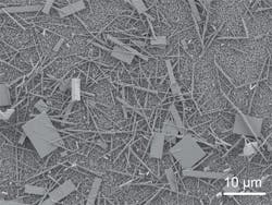
"While most researchers make these perovskite compounds into thin films for the fabrication of solar cells, we have developed an extremely simple method to grow them into elongated crystals that make extremely promising lasers," Jin says. The tiny nanometer-scale rectangular crystals grown in Jin's lab are called nanowires.
The new growth technique skips the costly, complicated equipment needed to make conventional lasers, says Jin, an expert on crystal growth and nanomaterial synthesis. He says the nanowires grow in about 20 hours once a glass plate coated with a solid reactant is submerged in a solution of the second reactant. "There's no heat, no vacuum, no special equipment needed," says Jin. "They grow in a beaker on the lab bench. The single-crystal perovskite nanowires grown from solutions at room temperature are high quality, almost free of defects, and they have the nice reflective parallel facets that a laser needs," Jin explains. "Most importantly, according to the conventional measures of lasing quality and efficiency, they are real standouts."
When tested in the lab of Jin's collaborator, Xiaoyang Zhu of Columbia University, the lasers were nearly 100% efficient. Essentially every photon absorbed produced a photon of laser light. "The advantage of these nanowire lasers is the much higher efficiency, by at least one order of magnitude, over existing ones," says Zhu.
Nanowire lasers have the potential to enhance efficiency and miniaturize devices, and could be used in devices that merge optical and electronic technology for computing, communication and sensors. "These are simply the best nanowire lasers by all performance criteria," says Jin, "even when compared to materials grown in high temperature and high vacuum. Perovskites are intrinsically good materials for lasing, but when they are grown into high-quality crystals with the proper size and shape, they really shine."
What is also exciting is that simply tweaking the recipe for growing the nanowires could create a series of lasers that emit a specific wavelength of light in many areas of the visible spectrum.
Before these nanowire lasers can be used in practical applications, Jin says their chemical stability must be improved. Also important is finding a way to stimulate the laser with electricity rather than light, which was just demonstrated.
The collaborative research was funded by the U.S. Department of Energy Basic Energy Sciences program. Graduate student Yongping Fu designed, synthesized and characterized the perovskite nanowires in Jin's lab in Madison. Haiming Zhu, a postdoctoral researcher in Zhu's lab at Columbia, carried out the optical studies of those nanowires and established their remarkable lasing properties.
SOURCE: University of Wisconsin-Madison; http://www.news.wisc.edu/23649

Gail Overton | Senior Editor (2004-2020)
Gail has more than 30 years of engineering, marketing, product management, and editorial experience in the photonics and optical communications industry. Before joining the staff at Laser Focus World in 2004, she held many product management and product marketing roles in the fiber-optics industry, most notably at Hughes (El Segundo, CA), GTE Labs (Waltham, MA), Corning (Corning, NY), Photon Kinetics (Beaverton, OR), and Newport Corporation (Irvine, CA). During her marketing career, Gail published articles in WDM Solutions and Sensors magazine and traveled internationally to conduct product and sales training. Gail received her BS degree in physics, with an emphasis in optics, from San Diego State University in San Diego, CA in May 1986.
