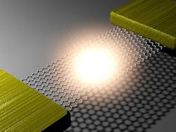
Graphene becomes incandescent light source for use in integrated photonic circuits
A team of scientists and engineers from Columbia University (New York, NY), Seoul National University (SNU; Seoul, South Korea), Korea Research Institute of Standards and Science (KRISS; Daejeon, South Korea) and the University of Texas at Austin have created an incandescent light source using graphene.1
A graphene strip spanning two conducting contacts placed on a silicon chip reaches temperatures of above 2500 °C, but its spectral output is not strictly a blackbody spectrum.
Spectral output of the heated graphene showed peaks at specific wavelengths, which the team discovered was due to interference between the light emitted directly from the graphene and light reflecting off the silicon substrate and passing back through the graphene. "This is only possible because graphene is transparent, unlike any conventional filament, and allows us to tune the emission spectrum by changing the distance to the substrate," notes Young Duck Kim, a Columbia University researcher.
As temperature goes up, conductivity goes down
The ability of graphene to achieve such high temperatures without melting the substrate or the metal electrodes results from the fact that, as it heats up, graphene becomes a much poorer conductor of heat; as a result, the high temperatures stay confined to a small "hot spot" in the center.
Light from the microscopic source is visible to the naked eye with no magnification.
The new type of light source could provide light within integrated photonic circuits and could possibly become a component of thin, flexible, transparent displays.
The team demonstrated the scalability of their technique by constructing large-scale arrays of chemical-vapor-deposited graphene light emitters.
The group is currently working to further characterize the performance of these devices -- for example, how fast they can be turned on and off -- and to develop techniques for integrating them into flexible substrates.
Sources:
http://engineering.columbia.edu/worlds-thinnest-light-bulb%E2%80%94graphene-gets-bright
http://news.utexas.edu/2015/06/15/researchers-build-worlds-thinnest-light-bulb-from-graphene
REFERENCE:
1. Young Duck Kim et al., Nature Nanotechnology (2015); http://dx.doi.org/10.1038/nnano.2015.118.

John Wallace | Senior Technical Editor (1998-2022)
John Wallace was with Laser Focus World for nearly 25 years, retiring in late June 2022. He obtained a bachelor's degree in mechanical engineering and physics at Rutgers University and a master's in optical engineering at the University of Rochester. Before becoming an editor, John worked as an engineer at RCA, Exxon, Eastman Kodak, and GCA Corporation.
