Zepler Institute manufactures record length of photonic bandgap fiber
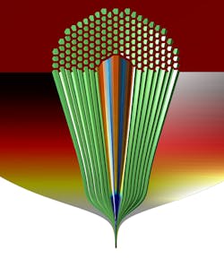
Image: Cut-away of a hollow core photonic bandgap fiber is shown neck down, as generated by a fluid dynamics simulation. The approximately 1 cm wide preform is drawn down to a slender approximately 0.2 mm fiber in a hot furnace under gravity and longitudinal tension. The outer glass is colored to show temperature (hottest region in white), while the microstructure is colored to show whether surface tension (blue) or differential pressure (red) forces dominate. (Image credit: Gregory Jasion, University of Southampton)
A photonic bandgap or microstructured fiber that supports > 200 nm bandwidth with a longitudinally uniform loss of 5 dB/km at 1560 nm was manufactured by researchers at the University of Southampton's Zepler Institute (Southampton, England). The 19 cell core and 5 cladding ring structure was unique not for its design, but for its length: it was manufactured in a record length of 11 km with low loss and maintaining its broad transmission bandwidth. Up to now, these fibers had only been made in lengths of hundreds of meters. The fiber was made using a conventional two-stage stack-and-draw technique.
RELATED ARTICLE: MSEM models holey fiber drawing process
"Hollow core photonic bandgap fibre has only had niche applications up until now because it was thought that it could not be manufactured in lengths suitable for telecoms applications," said Marco Petrovich, a senior member of the Zepler Institute team developing hollow core fiber technology with funding from both the UK Engineering and Physical Sciences Research Council and European Union FP7 programme. "Not only have we successfully made a photonic bandgap fibre in a suitable length, we have also engineered it to have the right properties for telecoms applications."
Petrovich and his colleagues have demonstrated that the fiber has error-free, low-latency, direct-detection 10Gbit/s transmission across the entire C-Band.
Manufacturing long lengths of microstructured fiber is notoriously difficult because unlike conventional fibers whose properties depend on the materials used to make them, the properties of photonic bandgap fibers depend on their structure. The nodes and struts that give photonic bandgap fiber its properties are usually on a sub-micron scale with many even just a few nanometers in size. “Any small change in these structures can change the properties along the fibre," said Petrovich. "We have shown that our fibre's properties are consistent along its entire length."
The breakthrough was made possible due to an improved understanding of fiber properties deriving from various new numerical and experimental fabrication and characterization tools recently developed by the team of researchers.
"We demonstrated data transmission at 10Gb/s along a 11km span using direct detection, showing only minor penalties and achieving an estimated > 15 μs latency reduction relative to standard fibre," said Petrovich. "Our numerical models of the fibre drawing process give us confidence that much longer fibre yields are feasible through further scaling of the process, and that much lower loss fibres should ultimately be possible."
SOURCE: University of Southampton; http://www.zeplerinstitute.com/news/4726
This article was published by Laser Focus World on 6/11/2015

Gail Overton | Senior Editor (2004-2020)
Gail has more than 30 years of engineering, marketing, product management, and editorial experience in the photonics and optical communications industry. Before joining the staff at Laser Focus World in 2004, she held many product management and product marketing roles in the fiber-optics industry, most notably at Hughes (El Segundo, CA), GTE Labs (Waltham, MA), Corning (Corning, NY), Photon Kinetics (Beaverton, OR), and Newport Corporation (Irvine, CA). During her marketing career, Gail published articles in WDM Solutions and Sensors magazine and traveled internationally to conduct product and sales training. Gail received her BS degree in physics, with an emphasis in optics, from San Diego State University in San Diego, CA in May 1986.
