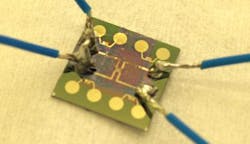
'Functionalized' graphene bonds closely with silicon to extract heat from photonic emitters
Researchers at Chalmers University of Technology (Göteborg, Sweden) have developed a method for efficiently cooling electronics using graphene-based film.1 The film has a thermal conductivity capacity that is four times that of copper. Moreover, the graphene film is attachable to photonic and electronic components made of silicon (Si), which improves the film's performance over that in previous, similar experiments on thermal cooling with graphene.
A couple of years ago, a research team led by Johan Liu, professor at Chalmers University of Technology, were the first to show that graphene can have a cooling effect on silicon-based devices. That was the starting point for researchers conducting research on this topic.
"But the methods that have been in place so far have presented the researchers with problems," Johan Liu says. "It has become evident that those methods cannot be used to rid electronic devices off great amounts of heat, because they have consisted only of a few layers of thermal conductive atoms. When you try to add more layers of graphene, another problem arises, a problem with adhesiveness. After having increased the amount of layers, the graphene no longer will adhere to the surface, since the adhesion is held together only by weak van der Waals bonds. We have now solved this problem by managing to create strong covalent bonds between the graphene film and the surface, which is an electronic component made of silicon."
The stronger bonds result from so-called functionalization of the graphene, i.e. the addition of a property-altering molecule. Having tested several different additives, the Chalmers researchers concluded that an addition of (3-Aminopropyl) triethoxysilane (APTES) molecules has the most desired effect. When heated and put through hydrolysis, it creates so-called silane bonds between the graphene and the electronic component.
Graphene versus diamond
Functionalization using silane coupling also increases the thermal conductivity of the graphene by 15% to 56%. The researchers have shown that the in-plane thermal conductivity of the graphene-based film, with 20 µm thickness, can reach a thermal conductivity value of 1600 W/m-K, which is four times that of copper. This is also greater than the thermal conductivity of diamond, which is about 1000 W/m-K; however, comparisons between cooling systems using these two carbon-based materials would have to take into effect the fact that diamond, although expensive, can be made in bulk pieces far thicker than 20 µm, thus increasing the diamond's total heat-conducting capacity.
"Increased thermal capacity could lead to several new applications for graphene," says Johan Liu. "One example is the integration of graphene-based film into microelectronic devices and systems, such as highly efficient LEDs, lasers, and radio-frequency components for cooling purposes."
Source: Chalmers University of Technology
REFERENCE:
1. Yong Zhang et al., Advanced Functional Materials (2015); doi: 10.1002/adfm.201500990

John Wallace | Senior Technical Editor (1998-2022)
John Wallace was with Laser Focus World for nearly 25 years, retiring in late June 2022. He obtained a bachelor's degree in mechanical engineering and physics at Rutgers University and a master's in optical engineering at the University of Rochester. Before becoming an editor, John worked as an engineer at RCA, Exxon, Eastman Kodak, and GCA Corporation.
