Perfect absorbers capture specific wavelengths from the visible to the near-infrared
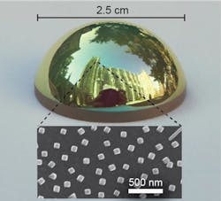
Researchers at Duke University (Durham, NC) have created a type of absorptive plasmonic metasurface based on silver nanocubes about 100 nm in size; the metasurface becomes a perfect absorber for a small band of the electromagnetic spectrum ranging from visible light through the near infrared.1 The fabrication technique is easily scalable, can be applied to any surface geometry, and costs much less than current light absorption technologies.
This sort of metasurface could allow advanced thermal imaging systems to not only be produced faster and cheaper than today's counterparts, but to have higher sensitivity. It could also be used in a variety of other applications, such as cloaking the heat signatures of objects.
"By borrowing well-known techniques from chemistry and employing them in new ways, we were able to obtain significantly better resolution than with a million-dollar state-of-the-art electron-beam lithography system," says Maiken Mikkelsen, the research team's leader. "This allowed us to create a coating that can fine-tune the absorption spectra with a level of control that hasn't been possible previously, with potential applications from light harvesting and photodetectors to military applications."
"This doesn't require top-down fabrication such as expensive lithography techniques and we don't make this in a clean room," notes Gleb Akselrod, a postdoctoral researcher in Mikkelsen's laboratory. "We build it from the bottom up, so the whole thing is inherently cheap and very scalable to large areas."
The researchers first coat a surface with a thin film of gold, then put down a few-nanometer-thin layer of polymer, followed by a coating of silver cubes about 100 nm in size. By controlling the thickness of the polymer film and the size and number of silver nanocubes, the coating can be tuned to absorb different wavelengths of light.
Coating photodetectors to absorb only specific wavelengths of infrared light would allow novel and cheap cameras to be made that could see different infrared colors.
In addition, if one can control the colors of light that a material absorbs, then one can also control the wavelengths of light that it emits; so by making the nanocubes larger to absorb wavelengths corresponding to thermal radiation, this technology could mask an object’s natural thermal radiation.
Source: http://pratt.duke.edu/news/new-technology-colors-infrared-rainbow
REFERENCE:
1. Gleb M. Akselrod et al., Advanced Materials (2015); doi: 10.1002/adma.201503281
About the Author
John Wallace
Senior Technical Editor (1998-2022)
John Wallace was with Laser Focus World for nearly 25 years, retiring in late June 2022. He obtained a bachelor's degree in mechanical engineering and physics at Rutgers University and a master's in optical engineering at the University of Rochester. Before becoming an editor, John worked as an engineer at RCA, Exxon, Eastman Kodak, and GCA Corporation.

