Xaar and Lawter collaborate to deliver silver nanoink printing for flexible optoelectronics
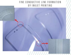
| With oven sintering or photonic curing, nanosilver conductive inks can produce lines with thickness below 1 µm. (Image: Lawter) |
A collaboration between industrial inkjet-printer specialist Xaar (Cambridge, England) and graphic-arts chemical maker Lawter (Chicago, IL), along with Lawter's parent company Harima Chemicals Group (HCG; Tokyo, Japan) has come together to improve nanosilver conductive inks as used by the Xaar inkjet-printer printhead. Conductive inks are a crucial part of some flexible-display designs, as well as other wearable and flexible photonics and electronics. Conductive ink can also enable wearable sensors and antennas.
According to the team members, inkjet is a cleaner process than other methods of printing silver inks, which is especially relevant when printing onto a substrate, such as a display, in which any yield loss is very expensive. With inkjet, manufacturers can precisely control the amount of ink dispensed in certain areas of a pattern so that the ink or fluid deposited can be thicker in some areas and thinner in others. Similarly, inkjet enables the deposition of a much thinner layer of fluids than traditional methods, which is significant for the manufacturers looking to produce thinner devices. In addition, inkjet is one of the few technologies able to print a circuit over a substrate that has a structured surface.
HCG developed and began the manufacture of silver nanoparticle conductive inks for the printed electronics industry 20 years ago and has more than 100 patents related to its low-temperature-sintered nanoparticle dispersion technology, which is cured by heat applied in a variety of ways, including by light ("photonic curing").
Xaar has been in the industrial inkjet business for 25 years.
Source: Xaar and Lawter
