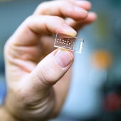
UCSC optofluidic platform uses flexible silicone for tunability and light control
The latest device from the lab of Holger Schmidt, electrical engineer at the University of California, Santa Cruz (UC Santa Cruz), combines high-performance microfluidics (also called optofluidics) for sample processing with dynamic optical tuning and switching, all on a low-cost "chip" made of a flexible silicone material.
RELATED ARTICLE: Optofluidics and the next generation of health-care engineering
In previous devices from Schmidt's lab, optical functions were built into silicon chips using the same fabrication technology used to make computer chips. The new device, described in Scientific Reports, is made entirely of polydimethylsiloxane (PDMS), a soft, flexible material used in microfluidics as well as in products such as contact lenses and medical devices.
"We can use this fabrication method now to build an all-in-one device that allows us to do biological sample processing and optical detection on one chip," said Schmidt, the Kapany Professor of Optoelectronics and director of the W. M. Keck Center for Nanoscale Optofluidics at UC Santa Cruz.
The flexibility of PDMS allows for novel ways of controlling both light and fluids on the chip. Using multilayer soft lithography techniques, senior graduate student Joshua Parks built chips containing both solid-core and hollow-core waveguides for guiding light signals, as well as fluidic microvalves to control the movement of liquid samples. Schmidt and Parks also developed a special microvalve that functions as a "lightvalve," controlling the flow of both light and fluids.
"That opens up a whole new set of functions that we couldn't do on a silicon chip," Schmidt said. "The lightvalve is the most exciting element. In additional to a simple on-off switch, we built a moveable optical trap for analysis of biological particles such as viruses or bacteria."
In a previous study, Schmidt, Parks, and colleagues at BYU and UC Berkeley demonstrated a hybrid device in which a PDMS microfluidic chip for sample preparation was integrated with a silicon-based optofluidic chip for optical detection of viral pathogens like ebola. The new device combines both functions on the same chip. In addition, Schmidt said, the materials are relatively inexpensive, allowing rapid prototyping of devices.
Schmidt said the potential applications for this technology include a wide range of biological sensors and analytical devices. For viral diagnostic assays, for example, fluorescently labeled antibodies can be used to tag specific viral strains for optical detection. Schmidt and colleagues demonstrated detection and identification of different flu strains using fluorescence detection in a multi-mode interference (MMI) waveguide. With the new device, they showed that they can actively tune an MMI waveguide on the chip.
The dynamic tuning of the optofluidic device is achieved by applying pressure to the optofluidic channel, changing its dimensions and thereby altering its photonic properties. "We can actually tune the spot pattern made in the channel by the interference waveguide, which we couldn't do with the silicon chip," Schmidt said.
SOURCE: UC Santa Cruz; https://www.soe.ucsc.edu/news/article/2433

Gail Overton | Senior Editor (2004-2020)
Gail has more than 30 years of engineering, marketing, product management, and editorial experience in the photonics and optical communications industry. Before joining the staff at Laser Focus World in 2004, she held many product management and product marketing roles in the fiber-optics industry, most notably at Hughes (El Segundo, CA), GTE Labs (Waltham, MA), Corning (Corning, NY), Photon Kinetics (Beaverton, OR), and Newport Corporation (Irvine, CA). During her marketing career, Gail published articles in WDM Solutions and Sensors magazine and traveled internationally to conduct product and sales training. Gail received her BS degree in physics, with an emphasis in optics, from San Diego State University in San Diego, CA in May 1986.
