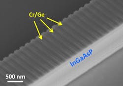
In a demonstration of two opposite functions at a frequency within the telecommunications band, scientists at the Department of Energy's Lawrence Berkeley National Laboratory (Berkeley Lab; Berkeley, CA) have for the first time created a single device that acts as both a laser and an anti-laser. Reported in Nature Photonics, the research lays the groundwork for developing a new type of integrated device with the flexibility to operate as a laser, an amplifier, a modulator, and an absorber or detector.
RELATED ARTICLE: Yale 'anti-laser' absorbs light
"In a single optical cavity we achieved both coherent light amplification and absorption at the same frequency, a counterintuitive phenomenon because these two states fundamentally contradict each other," said study principal investigator Xiang Zhang, senior faculty scientist at Berkeley Lab's Materials Sciences Division. "This is important for high-speed modulation of light pulses in optical communication."
The concept of anti-lasers, or coherent perfect absorbers (CPAs), emerged in recent years as something that reverses what a laser does. Instead of strongly amplifying a beam of light, an anti-laser can completely absorb incoming coherent light beams. First demonstrated five years ago by Yale University researchers, anti-lasers are still being explored. Because anti-lasers can pick up weak coherent signals in the midst of a “noisy” incoherent background, they could be used as an extremely sensitive chemical or biological detector.
The researchers used nanofabrication technology to build 824 repeating pairs of gain and loss materials to form the device, which measured 200 micrometers long and 1.5 micrometers wide. The gain medium was made out of indium gallium arsenide phosphide, a well-known material used as an amplifier in optical communications. Chromium paired with germanium formed the loss medium. Repeating the pattern created a resonant system in which light bounces back and forth throughout the device to build up the amplification or absorption magnitude.
If one is to send light through such a gain-loss repeating system, an educated guess is that light will experience equal amounts of amplification and absorption, and the light will not change in intensity. However, this is not the case if the system satisfies conditions of parity-time symmetry, which is the key requirement in the device design.
Soon after the discovery of the anti-laser, scientists had predicted that a system exhibiting parity-time symmetry could support both lasers and anti-lasers at the same frequency in the same space. In the device created by Zhang and his group, the magnitude of the gain and loss, the size of the building blocks, and the wavelength of the light moving through combine to create conditions of parity-time symmetry.
In experiments, two light beams of equal intensity were directed into opposite ends of the device. The researchers found that by tweaking the phase of one light source, they were able to control whether the light waves spent more time in amplifying or absorbing materials. If the phase of the two wavelengths is equal and they enter the device at the same time, there is neither amplification nor absorption because the light spends equal time in each region. The researchers targeted a wavelength of about 1556 nm, which is within the band used for optical telecommunications.
"This work is the first demonstration of balanced gain and loss that strictly satisfies conditions of parity-time symmetry, leading to the realization of simultaneous lasing and anti-lasing," said study co-author Liang Feng, former postdoctoral researcher in Zhang's Lab, and now an assistant professor of electrical engineering at the University at Buffalo. "The successful attainment of both lasing and anti-lasing within a single integrated device is a significant step towards the ultimate light control limit."
SOURCE: Berkeley Lab; http://newscenter.lbl.gov/2016/11/07/lasers-anti-lasers-one-device/

Gail Overton | Senior Editor (2004-2020)
Gail has more than 30 years of engineering, marketing, product management, and editorial experience in the photonics and optical communications industry. Before joining the staff at Laser Focus World in 2004, she held many product management and product marketing roles in the fiber-optics industry, most notably at Hughes (El Segundo, CA), GTE Labs (Waltham, MA), Corning (Corning, NY), Photon Kinetics (Beaverton, OR), and Newport Corporation (Irvine, CA). During her marketing career, Gail published articles in WDM Solutions and Sensors magazine and traveled internationally to conduct product and sales training. Gail received her BS degree in physics, with an emphasis in optics, from San Diego State University in San Diego, CA in May 1986.
